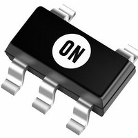
NCP1550SN25T1 ON Semiconductor, NCP1550SN25T1 Datasheet - Page 13

NCP1550SN25T1
Manufacturer Part Number
NCP1550SN25T1
Description
IC CTR PFM/PWM DCDC 2.5V TSOT235
Manufacturer
ON Semiconductor
Datasheet
1.NCP1550SN18T1.pdf
(17 pages)
Specifications of NCP1550SN25T1
Pwm Type
Voltage Mode
Number Of Outputs
1
Frequency - Max
690kHz
Duty Cycle
100%
Voltage - Supply
2.45 V ~ 5.5 V
Buck
Yes
Boost
No
Flyback
No
Inverting
No
Doubler
No
Divider
No
Cuk
No
Isolated
No
Operating Temperature
-40°C ~ 85°C
Package / Case
TSOT-23-5, TSOT-5, TSOP-5
Frequency-max
690kHz
Mounting Style
SMD/SMT
Lead Free Status / RoHS Status
Contains lead / RoHS non-compliant
Other names
NCP1550SN25T1OSTR
Available stocks
Company
Part Number
Manufacturer
Quantity
Price
Part Number:
NCP1550SN25T1G
Manufacturer:
ON/安森美
Quantity:
20 000
Detailed Operating Description
controllers designed primarily for use in portable
applications powered by battery cells. With an appropriate
external P−channel MOSFET connected, the device can
provide up to 2 A loading current with high conversion
efficiency. The NCP1550 series using an unique control
scheme combines the advantages of Pulse−Frequency−
Modulation (PFM) that can provide excellent efficiency
even at light loading conditions and Constant−Frequency
Pulse−Width−Modulation that can achieve high efficiency
and low output voltage ripple at heavy loads. The NCP1550
working at high switching frequency makes it possible to use
small size surface mount inductor and capacitors to reduce
PCB area and provide better interference handling for noise
sensitive applications. The simplified functional blocks of
the device are shown in Figure 1 and descriptions for each
of the functions are given below.
The Internal Oscillator
cycles is required. NCP1550 have an internal Fixed−
Frequency oscillator. The oscillator frequency is trimmed to
600 kHz with an accuracy of ±15%. All other timing signals
needed for operation are derived from this oscillator signal.
Voltage Reference and Soft−Start
NCP1550. This reference voltage is connected to the
inverting input terminal of the error amplifier, A1, which
compared with portion of the output voltage, V
from an integrated voltage divider with precise trimming to
give the required output voltage at ±2% accuracy. NCP1550
also comes with a built−in soft−start circuit that controls the
ramping up of the internal reference voltage during the
power−up of the converter. This function effectively enables
the output voltage to rise gradually over the specified
soft−start time, 8 msec typical. This prevents the output
voltage from overshooting during startup of the converter.
Voltage Mode Pulse−Width−Modulation (PWM)
Control Scheme
Constant−Frequency
Voltage Mode Control. The controller operates with the
internal oscillator, which generates the required ramp
function to compare with the output of the error amplifier, A1.
The error amplifier compares the internally divided−down
output voltage with the voltage reference to produce an error
The NCP1550 series are step−down (Buck) DC−DC
An oscillator that governs the switching of a PWM control
An internal high accuracy voltage reference is included in
For normal operation, NCP1550 is working in
Pulse−Width−Modulation
DETAILED OPERATING DESCRIPTION
OUT
derived
(PWM)
http://onsemi.com
NCP1550
13
voltage at its output. This error voltage is compared with the
ramp function to generate the control pulse to drive the
external power switch. On a cycle−by−cycle basis, the
greater the error voltage, the longer the switch is held on.
Hence, corresponding corrective action will be made to keep
the output voltage within regulation. Constant−Frequency
PWM reduces output voltage ripple and noise, which is one
of the important characteristics for noise sensitive
communication applications. The high switching frequency
allows small size surface mount components to improve
layout compactness and reduce PC board area, and eliminate
audio and emission interference.
Power−Saving Pulse−Frequency−Modulation (PFM)
Control Scheme
Discontinuous Conduction Mode (DCM) operation, which
means the inductor current will decrease to zero before the
next switching cycle starts. In DCM operation, the ON time
for each switching cycle will decrease significantly when
the output current decreases. In order to maintain a high
conversion efficiency even at light load conditions, the ON
time for each switching cycle is closely monitored and for
any ON time smaller than the preset value, 320 nsec, the
switching pulse will be skipped. As a result, when the
loading current is small, the converter will be operating in a
“Constant ON time (320 nsec nominal), variable OFF time”
Pulse−Frequency Modulation (PFM) mode. This innovative
control scheme improves the conversion efficiency for the
system at light load and standby operating conditions hence
extend the operating life of the battery.
Low Power Shutdown Mode
tied to GND. In shutdown, the internal reference, oscillator,
control circuitry, driver and internal feedback voltage
divider are turned off and the output voltage falls to 0 V.
During the shutdown mode, as most of the internal functions
are stopped and current paths are cut−off, the device
consume extremely small current in this condition.
Under−Voltage Lockout (UVLO)
safe input voltage levels, an Undervoltage Lockout is
incorporated into the NCP1550. When the input supply
voltage drops below approximately 2.2 V, the comparator,
CP1 will turn−off the control circuitry and shut the converter
down.
While the loading is decreasing, the converter enters the
NCP1550 can be disabled whenever the CE pin (Pin 1) is
To prevent operation of the P−Channel MOSFET below


