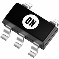
NCP1550SN25T1 ON Semiconductor, NCP1550SN25T1 Datasheet - Page 15

NCP1550SN25T1
Manufacturer Part Number
NCP1550SN25T1
Description
IC CTR PFM/PWM DCDC 2.5V TSOT235
Manufacturer
ON Semiconductor
Datasheet
1.NCP1550SN18T1.pdf
(17 pages)
Specifications of NCP1550SN25T1
Pwm Type
Voltage Mode
Number Of Outputs
1
Frequency - Max
690kHz
Duty Cycle
100%
Voltage - Supply
2.45 V ~ 5.5 V
Buck
Yes
Boost
No
Flyback
No
Inverting
No
Doubler
No
Divider
No
Cuk
No
Isolated
No
Operating Temperature
-40°C ~ 85°C
Package / Case
TSOT-23-5, TSOT-5, TSOP-5
Frequency-max
690kHz
Mounting Style
SMD/SMT
Lead Free Status / RoHS Status
Contains lead / RoHS non-compliant
Other names
NCP1550SN25T1OSTR
Available stocks
Company
Part Number
Manufacturer
Quantity
Price
Part Number:
NCP1550SN25T1G
Manufacturer:
ON/安森美
Quantity:
20 000
PCB Layout Recommendations
mode power conversion. Careful PCB layout can help to
minimize ground bounce, EMI noise and unwanted
feedbacks that can affect the performance of the converter.
Suggested hints below can be used as a guideline in most
situations.
Grounding
output power return ground, the input power return ground
and the device power ground together at one point. All high
current running paths must be thick enough for current
flowing through and producing insignificant voltage drop
along the path. Feedback signal path must be separated from
the main current path and sensing directly at the anode of the
output capacitor.
External Component Reference Data
NCP1550SN18T1
NCP1550SN19T1
NCP1550SN25T1
NCP1550SN27T1
NCP1550SN30T1
NCP1550SN33T1
Good PCB layout plays an important role in switching
Star−ground connection should be used to connect the
Device
V
1.8 V
1.9 V
2.5 V
2.7 V
3.0 V
3.3 V
OUT
CDD5D23
CDRH6D38 6R8 (2A)
Sumida
CDC5D23
CDRH6D38 6R8 (2A)
Sumida
CDC5D23
CDRH6D38 5R0 (2A)
Sumida
CDC5D23
CDRH6D38 5R0 (2A)
Sumida
CDC5D23
CDRH6D28 5R0 (2A)
Sumida
CD43
CDRH6D38 3R3 (2A)
Sumida
Inductor Model
6R8 (1A)
6R8 (1A)
5R6 (1A)
5R6 (1A)
4R7 (1A)
3R3 (1A)
Inductor
6.8 mH
6.8 mH
5.6 mH
5.0 mH
5.6 mH
5.0 mH
5.6 mH
5.0 mH
3.3 mH
http://onsemi.com
(L)
NCP1550
15
ON Semiconductor
ON Semiconductor
ON Semiconductor
ON Semiconductor
ON Semiconductor
ON Semiconductor
External MOSFET
NTGS3441T1 (1A)
NTGS3443T1 (2A)
NTGS3441T1 (1A)
NTGS3443T1 (2A)
NTGS3441T1 (1A)
NTGS3443T1 (2A)
NTGS3441T1 (1A)
NTGS3443T1 (2A)
NTGS3441T1 (1A)
NTGS3443T1 (2A)
NTGS3441T1 (1A)
NTGS3443T1 (2A)
Components Placement
output capacitor, must be placed as close together as possible.
All connecting traces must be short, direct and thick. High
current flowing and switching paths must be kept away from
the feedback (V
injection of noise into the feedback path.
Feedback Path
separated from the power path. The output voltage sensing
trace to the feedback (V
to the output voltage directly at the anode of the output
capacitor.
Power components, i.e. input capacitor, inductor and
Feedback of the output voltage must be a separate trace
(M)
OUT
MBRM120LT3
ON Semiconductor
MBRM120LT3
ON Semiconductor
MBRM120LT3
ON Semiconductor
MBRM120LT3
Semiconductor
MBRM120LT3
ON Semiconductor
MBRM120LT3
ON Semiconductor
, pin 3) terminal to avoid unwanted
OUT
Diode
(SD)
, pin 3) pin should be connected
33 mF/33 mF (1A)
68 mF/33 mF (2A)
KEMET
(T494 series)
33 mF/33 mF (1A)
68 mF/33 mF (2A)
KEMET
(T494 series)
33 mF/33 mF (1A)
68 mF/33 mF (2A)
KEMET
(T494 series)
33 mF/33 mF (1A)
68 mF/33 mF (2A)
KEMET
(T494 series)
33 mF/33 mF (1A)
68 mF/33 mF (2A)
KEMET
(T494 series)
68 mF/33 mF (1A)
100 mF/68 mF (2A)
KEMET
(T494 series)
Output and Input
Capacitor
C
OUT
/C
IN


