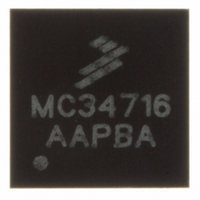
MC34716EP Freescale Semiconductor, MC34716EP Datasheet - Page 12

MC34716EP
Manufacturer Part Number
MC34716EP
Description
IC CONVERTER DDR 26QFN
Manufacturer
Freescale Semiconductor
Datasheet
1.MC34716EP.pdf
(27 pages)
Specifications of MC34716EP
Applications
Converter, DDR
Voltage - Input
3 ~ 6 V
Number Of Outputs
2
Voltage - Output
0.7 ~ 3.6 V
Operating Temperature
-40°C ~ 85°C
Mounting Type
Surface Mount
Package / Case
26-QFN
Output Voltage
0.7 V to 3.6 V
Output Current
5 A
Input Voltage
3 V to 6 V
Switching Frequency
1 MHz
Operating Temperature Range
- 40 C to + 85 C
Mounting Style
SMD/SMT
Lead Free Status / RoHS Status
Lead free / RoHS Compliant
Available stocks
Company
Part Number
Manufacturer
Quantity
Price
Part Number:
MC34716EP
Manufacturer:
FREESCALE
Quantity:
20 000
commands and control lines require system level termination
to a voltage (V
(V
supply insures symmetry for switching times. Also, a
reference voltage (V
variations is needed for the DDR SDRAM input receiver,
V
effect the setup and hold time of the memory. To comply with
DDR requirements and to obtain best performance, V
V
voltage, temperature, and noise margins. V
any variations in the DC V
(See
output. To ensure compliance with DDR specifications, the
V
internally through a precision resistor divider. This internal
voltage is then used as the reference voltage for the V
output. The same internal voltage is also buffered to give the
V
without the need for an external resistor divider. The 34716
provides the tight voltage regulation and power sequencing/
tracking required along with handling the DDR peak transient
current requirements. It gives the user a complete DDR
power supply solution with optimum performance. Buffering
the V
changes.
switching converter topology with integrated low R
(50 mΩ) N-channel power MOSFETs to provide an output
voltage with an accuracy of less than ±2.0% output voltage.
It has a programmable switching frequency that allows for
flexibility and optimization over the operating conditions and
can operate at up to 1.0 MHz to significantly reduce the
external components size and cost. The 34716 can supply up
to 5.0 A from one output and sink and source up to 3.0 A of
BOOTSTRAP INPUT (BOOT1, BOOT2)
discussed in
pin and the SW pin of the respective channel to enhance the
gate of the high-side Power MOSFET during switching.
POWER INPUT VOLTAGE (PVIN1, PVIN2)
buck converter high side power MOSFET.
12
34716
FUNCTIONAL DESCRIPTION
INTRODUCTION
REF
REF
DDQ
REF
DDQ
In modern microprocessor/memory applications, address
The 34716 supplies the V
The 34716 utilizes a voltage mode synchronous buck
Bootstrap capacitor input pin. Connect a capacitor (as
Buck converter power input voltage. This is the drain of the
REF
is also equal to 1/2 V
Figure
need to be tightly regulated to track 1/2 V
voltage at the VREFOUT pin for the application to use
). Having the termination voltage at midpoint, the power
line is applied to the VREFIN pin and divided by 2
output helps its immunity against noise and load
6) for a DDR system level diagram.
Bootstrap capacitor on page
TT
) equal to 1/2 the memory supply voltage
REF
) that is free of any noise or voltage
REF
DDQ
DDQ
. Varying the V
value (V
, V
TT
and a buffered V
TT
= V
21) between this
FUNCTIONAL DESCRIPTION
TT
FUNCTIONAL PIN DESCRIPTION
REF
REF
should track
DDQ
+/- 40 mV),
voltage will
DS(ON)
across
TT
INTRODUCTION
TT
REF
and
continuous current from the other output. It provides
protection against output over-current, over-voltage, under-
voltage, and over-temperature conditions. It also protects the
system from short circuit events. It incorporates a power good
output signal to alert the host when a fault occurs.
the Suspend-To-Disk (S5) states, the 34716 offers the STBY
and the SD pins respectively. Pulling any of these pins low,
puts the IC in the corresponding state.
the Power MOSFET switches for the buck converter into a
space-efficient package, the 34716 offers a complete, small-
size, cost-effective, and simple solution to satisfy the needs
of DDR memory applications.
to supply termination for other active buses and graphics card
memory. It can be used in Netcom/Telecom applications like
servers. It can also be used in desktop motherboards, game
consoles, set top boxes, and high end high definition TVs.
SWITCHING NODE (SW1, SW2)
the output inductor.
POWER GROUND (PGND1, PGND2)
is the source of the buck converter low side power MOSFET.
COMPENSATION INPUT (COMP1, COMP2)
to this pin. Use a type III compensation network.
DDR Memory Controller
For boards that support the Suspend-To-RAM (S3) and
By integrating the control/supervisory circuitry along with
Besides DDR memory termination, the 34716 can be used
Buck converter switching node. This pin is connected to
Buck converter and discharge MOSFETs power ground. It
Buck converter external compensation network connects
V
DDQ
Figure 6. DDR System Level Diagram
R
S
BUS
Analog Integrated Circuit Device Data
R
T
V
TT
DDR Memory Input Receiver
Freescale Semiconductor
V
DDQ
V
REF


