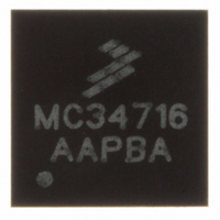
MC34716EP Freescale Semiconductor, MC34716EP Datasheet - Page 16

MC34716EP
Manufacturer Part Number
MC34716EP
Description
IC CONVERTER DDR 26QFN
Manufacturer
Freescale Semiconductor
Datasheet
1.MC34716EP.pdf
(27 pages)
Specifications of MC34716EP
Applications
Converter, DDR
Voltage - Input
3 ~ 6 V
Number Of Outputs
2
Voltage - Output
0.7 ~ 3.6 V
Operating Temperature
-40°C ~ 85°C
Mounting Type
Surface Mount
Package / Case
26-QFN
Output Voltage
0.7 V to 3.6 V
Output Current
5 A
Input Voltage
3 V to 6 V
Switching Frequency
1 MHz
Operating Temperature Range
- 40 C to + 85 C
Mounting Style
SMD/SMT
Lead Free Status / RoHS Status
Lead free / RoHS Compliant
Available stocks
Company
Part Number
Manufacturer
Quantity
Price
Part Number:
MC34716EP
Manufacturer:
FREESCALE
Quantity:
20 000
MODES OF OPERATION
Normal Mode
operational. To be in this mode, the V
operating range, both Shutdown and Standby inputs are
high, and no faults are present. This mode consumes the
most amount of power.
Standby Mode
solutions where the DDR supply is desired to be ACPI
compliant (Advanced Configuration and Power Interface).
When this mode is activated by pulling the STBY pin low, V
is put in High Z state, I
active. This is the S3 state Suspend-To-Ram or Self Refresh
mode and it is the lowest DRAM power state. In this mode,
the DRAM will preserve the data. While in this mode, the
34716 consumes less power than in the normal mode,
because the buck converter and most of the internal blocks
are disabled.
16
34716
FUNCTIONAL DEVICE OPERATION
OPERATIONAL MODES
T
The 34716 has three primary modes of operation:
In normal mode, all functions and outputs are fully
This mode is predominantly used in Desktop memory
V
J
TT
>= 170°C
I
For>=10 ms
>=V
OUT2
OVR2
>=I
Thermal Shutdown
V
LIM2
TT
Channel 2
V
V
Over-voltage
V
<=V
DDQ
PG = 1
REF
TT
V
V
V
PG = 1
DDQ
REF
=OFF
TT
UVF2
V
=ON
=ON
TT
=ON
=ON
=ON
Under-voltage
OUT2
Over-current
TIMEOUT=1
V
Channel 2
V
V
V
V
V
PG = 1
T
T
DDQ
REF
DDQ
PG = 1
REF
TT
TT
J
IMEOUT
V
<=145°C
=ON
V
V
=OFF
TT
= 0 A while V
=ON
=ON
=ON
TT2
=ON
TT
=>=V
T
Expired
<=V
IMEOUT
Expired
SD = 0 &
STBY=x
OVF2
UVR2
IN
FUNCTIONAL DEVICE OPERATION
needs to be within its
V
V
V
DDQ
DDQ
REF
TT
Shutdown
= Discharge
PG = 1
= Discharge
Figure 8. Operation Modes Diagram
= Discharge
SD = 1 &
STBY=1
I
OUT2
and V
Short-circuit
TIMEOUT=1
T
Expired
V
V
V
IMEOUT
OUT2
OUT1
OPERATIONAL MODES
PG = 1
>=I
REF
V
REF
TT
SHORT2
=OFF
=ON
=ON
V
F
I
stay
LM1
DDQ
3.0 V<=V
SW
V
TT
IN
V
is programmed
is programmed
V
V
and V
< 3.0 V
DDQ
Normal
PG = 0
TT
REF
= ON
=ON
IN
= ON
TT
<=6.0 V
t
Shutdown Mode
is in a shutdown state and the outputs are all disabled and
discharged. This is the S4/S5 power state or Suspend-To-
Disk state, where the DRAM will loose all of its data content
(no power supplied to the DRAM). The reason to discharge
the V
shutdown mode that V
otherwise V
V
the least amount of power since almost all of the internal
blocks are disabled.
START-UP SEQUENCE
of the SD and STBY pins. If the device is in a shutdown mode,
no block will power up and the output will not attempt to ramp.
If the device is in a standby mode, only the V
supply voltage and the bias currents are established and no
further activities will occur. Once the SD and STBY pins are
released to enable the device, the internal V
also released. The rest of the internal blocks will be enabled,
and the buck converters switching frequency and the V
ss
DDQ
= 1
V
V
Short-circuit
Power Off
In this mode, activated by pulling the SD pin low, the chip
When power is first applied, the 34716 checks the status
TIMEOUT=1
V
V
DDQ
REF
PG = 1
V
TT
T
Expired
DDQ
V
PG = 1
REF
I
TT
IMEOUT
V
OUT1
TT
upon powering up. In this mode, the 34716 consumes
=OFF
=OFF
=OFF
DDQ
=ON
=OFF
=ON
and V
>=I
SD = 1 &
STBY=1
SHORT1
TT
REF
can remain floating high, and be higher than
lines is to ensure upon exiting, the
V
V
V
Standby
DDQ
REF
PG = 1
TT
V
TT
Analog Integrated Circuit Device Data
T
Expired
=OFF
DDQ
V
=OFF
IMEOUT
=ON
T
T
DDQ
and V
J
IMEOUT
<=145°C
<= V
Over-current
>= V
TIMEOUT=1
V
Channel 1
V
DDQ
V
OVF1
PG = 1
REF
SD = 1 &
STBY=0
TT
REF
Expired
UVR1
=ON
=OFF
=ON
Under-voltage
Freescale Semiconductor
are lower than V
V
V
V
DDQ
PG = 1
REF
TT2
Thermal Shutdown
V
DDQ
Over-voltage
=ON
=ON
=ON
V
V
Channel 1
V
V
V
DDQ
V
DDQ
PG = 1
OTT
REF
PG = 1
REF
V
TT
DDI
V
DDQ
=ON
DDQ
=ON
=ON
=OFF
=ON
=ON
DDI
POR signal is
V
I
For>=10 ms
<=V
DDQ
OUT1
internal
T
UVF1
>=V
J
DDQ
>=I
>=170°C
OVR1
LIM1
DDQ
,


