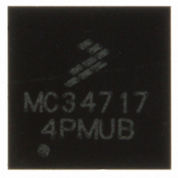
MC34717EP Freescale Semiconductor, MC34717EP Datasheet - Page 7

MC34717EP
Manufacturer Part Number
MC34717EP
Description
IC CONVERTER DDR 26QFN
Manufacturer
Freescale Semiconductor
Datasheet
1.MC34717EP.pdf
(28 pages)
Specifications of MC34717EP
Applications
Converter, DDR
Voltage - Input
3 ~ 6 V
Number Of Outputs
2
Voltage - Output
0.7 ~ 3.6 V
Operating Temperature
-40°C ~ 85°C
Mounting Type
Surface Mount
Package / Case
26-QFN
Output Voltage
0.7 V to 3.6 V
Output Current
5 A
Input Voltage
3 V to 6 V
Switching Frequency
1 MHz
Operating Temperature Range
- 40 C to + 85 C
Mounting Style
SMD/SMT
No. Of Outputs
2
Power Dissipation Pd
2.03W
No. Of Pins
26
Filter Terminals
SMD
Rohs Compliant
Yes
Lead Free Status / RoHS Status
Lead free / RoHS Compliant
Available stocks
Company
Part Number
Manufacturer
Quantity
Price
Part Number:
MC34717EP
Manufacturer:
FREESCALE
Quantity:
20 000
Table 3. Static Electrical Characteristics
values noted reflect the approximate parameter means at T
Analog Integrated Circuit Device Data
Freescale Semiconductor
IC INPUT SUPPLY VOLTAGE (VIN)
INTERNAL SUPPLY VOLTAGE OUTPUT (VDDI)
CHANNEL 1 BUCK CONVERTER (PVIN1, SW1, PGND1, BOOT1, INV1, COMP1, ILIM1)
Notes
Input Supply Voltage Operating Range
Input DC Supply Current
(Normal Mode: SD = 1, Unloaded Outputs)
Input DC Supply Current
(Shutdown Mode, SD = 0)
Internal Supply Voltage Range
Channel 1 High Side MOSFET Drain Voltage Range
Output Voltage Adjustment Range
Output Voltage Accuracy
Line Regulation
(Normal Operation, V
Load Regulation
(Normal Operation, I
Error Amplifier Reference Voltage
Output Under-voltage Threshold
Output Over-voltage Threshold
Continuous Output Current
Over-current Limit
Soft Start Adjusting Reference Voltage Range
Short-circuit Current Limit
High Side N-CH Power MOSFET (M4) R
(I
Low Side N-CH Power MOSFET (M5) R
(I
M2 R
(V
11.
12.
13.
Characteristics noted under conditions 3.0 V ≤ V
OUT1
OUT1
IN
= 3.3 V, M2 is on)
DS(ON)
Section “MODES OF OPERATION”, page
Design information only, this parameter is not production tested.
This is directly affected by the accuracy of the external feedback network, 1% feedback resistors are recommended.
= 1.0 A, V
= 1.0 A, V
(12)
(12)
BOOT1
IN
= 3.3 V)
OUT1
IN
- V
= 3.0 to 6.0 V, I
(11)
(11)
(12),(13)
= 0.0 to 5.0 A)
SW1
Characteristic
= 3.3 V)
(12)
(12)
OUT1
DS(ON)
DS(ON)
STATIC ELECTRICAL CHARACTERISTICS
= 2.5 A)
(12)
(12)
16
has a detailed description of the different operating modes of the 34717
IN
≤ 6.0 V, - 40°C ≤ T
A
= 25°C under nominal conditions, unless otherwise noted.
R
R
R
Symbol
V
REG
REG
DS(ON)HS1
I
DS(ON)LS1
DS(ON)M2
SHORT1
V
V
I
V
V
I
OUTHI1
INOFF
V
I
P
OUT1
A
V
REF1
UVR1
OVR1
LIM1
ILIM1
I
DDI
VIN
IN
-
IN
≤ 85°C, GND = 0 V, unless otherwise noted. Typical
LN1
LD1
2.35
1.25
Min
-1.0
-1.0
-1.0
-8.0
3.0
2.5
0.7
1.5
2.0
10
10
STATIC ELECTRICAL CHARACTERISTICS
-
-
-
-
-
-
ELECTRICAL CHARACTERISTICS
Typ
2.5
0.7
6.5
8.5
-
-
-
-
-
-
-
-
-
-
-
-
-
-
-
V
Max
2.65
-1.5
100
6.0
6.0
3.6
1.0
1.0
1.0
8.0
5.0
4.0
35
50
50
DDI
-
-
-
Unit
mΩ
mΩ
mA
µA
%
%
%
%
%
V
V
V
V
V
A
A
V
A
Ω
34717
7


