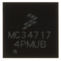
MC34717EP Freescale Semiconductor, MC34717EP Datasheet - Page 8

MC34717EP
Manufacturer Part Number
MC34717EP
Description
IC CONVERTER DDR 26QFN
Manufacturer
Freescale Semiconductor
Datasheet
1.MC34717EP.pdf
(28 pages)
Specifications of MC34717EP
Applications
Converter, DDR
Voltage - Input
3 ~ 6 V
Number Of Outputs
2
Voltage - Output
0.7 ~ 3.6 V
Operating Temperature
-40°C ~ 85°C
Mounting Type
Surface Mount
Package / Case
26-QFN
Output Voltage
0.7 V to 3.6 V
Output Current
5 A
Input Voltage
3 V to 6 V
Switching Frequency
1 MHz
Operating Temperature Range
- 40 C to + 85 C
Mounting Style
SMD/SMT
No. Of Outputs
2
Power Dissipation Pd
2.03W
No. Of Pins
26
Filter Terminals
SMD
Rohs Compliant
Yes
Lead Free Status / RoHS Status
Lead free / RoHS Compliant
Available stocks
Company
Part Number
Manufacturer
Quantity
Price
Part Number:
MC34717EP
Manufacturer:
FREESCALE
Quantity:
20 000
Table 3. Static Electrical Characteristics
values noted reflect the approximate parameter means at T
8
34717
ELECTRICAL CHARACTERISTICS
STATIC ELECTRICAL CHARACTERISTICS
CHANNEL 2 BUCK CONVERTER (PVIN2, SW2, PGND2, BOOT2, INV2, COMP2, ILIM2)
Notes
SW1 Leakage Current (Standby and Shutdown modes)
PVIN1 Pin Leakage Current
(Shutdown Mode)
Error Amplifier DC Gain
Error Amplifier Unit Gain Bandwidth
Error Amplifier Slew Rate
Error Amplifier Input Offset
INV1 Pin Leakage Current
Thermal Shutdown Threshold
Thermal Shutdown Hysteresis
Channel 2 High Side MOSFET Drain Voltage Range
Output Voltage Adjustment Range
Output Voltage Accuracy
Line Regulation
(Normal Operation, V
Load Regulation
(Normal Operation, I
Error Amplifier Reference Voltage
Output Under-voltage Threshold
Output Over-voltage Threshold
Continuous Output Current
Over-current Limit
Soft Start Adjusting Reference Voltage Range
Short-circuit Current Limit
High Side N-CH Power MOSFET (M6) R
(I
Low Side N-CH Power MOSFET (M7) R
(I
M3 R
(V
SW2 Leakage Current (Standby and Shutdown modes)
PVIN2 Pin Leakage Current
(Shutdown Mode)
14.
15.
16.
Characteristics noted under conditions 3.0 V ≤ V
OUT2
OUT2
IN
= 3.3 V, M3 is on)
DS(ON)
Design information only, this parameter is not production tested.
This is directly affected by the accuracy of the external feedback network, 1% feedback resistors are recommended.
±1% is assured at room temperature
= 1.0 A, V
= 1.0 A, V
(14)
(14)
BOOT2
IN
= 3.3 V)
OUT2
IN
- V
(14)
= 3.0 to 6.0 V, I
(14),(15),(16)
(14)
= 0.0 to 5.0 A)
SW2
(14)
Characteristic
(14)
(14)
= 3.3 V)
(14)
(14)
(14)
OUT2
DS(ON)
DS(ON)
= 2.5 A)
(14)
(14)
IN
≤ 6.0 V, - 40°C ≤ T
A
= 25°C under nominal conditions, unless otherwise noted.
R
OFFSET
R
T
R
UGBW
Symbol
T
SDHYFET1
V
REG
REG
DS(ON)HS2
I
DS(ON)LS2
DS(ON)M3
SHORT2
V
V
V
V
I
I
SR
SDFET1
I
OUTHI2
PVIN1
I
I
PVIN2
P
OUT2
A
A
I
I
INV1
REF2
UVR2
OVR2
LIM2
ILIM2
SW
SW
VIN
EA
-
EA
≤ 85°C, GND = 0 V, unless otherwise noted. Typical
LN2
LD2
EA
EA
1.25
Min
-3.0
-1.0
-1.0
-1.0
-1.0
-8.0
-10
-10
2.5
0.7
1.5
2.0
-10
-10
10
10
-
-
-
-
-
-
-
-
-
Analog Integrated Circuit Device Data
Typ
150
170
3.0
7.0
0.7
6.5
8.5
25
0
-
-
-
-
-
-
-
-
-
-
-
-
-
-
-
-
-
Freescale Semiconductor
V
Max
-1.5
3.0
1.0
6.0
3.6
1.0
1.0
1.0
8.0
5.0
4.0
10
10
50
50
10
10
DDI
-
-
-
-
-
-
-
-
MHz
Unit
V/µs
mΩ
mΩ
mV
µA
µA
dB
µA
°C
°C
µA
%
%
%
%
%
V
V
V
A
A
V
A
Ω
A


