LP2996LQ/NOPB National Semiconductor, LP2996LQ/NOPB Datasheet - Page 3
LP2996LQ/NOPB
Manufacturer Part Number
LP2996LQ/NOPB
Description
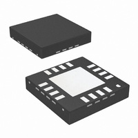
IC DDR TERMINATION REG 16LLP
Manufacturer
National Semiconductor
Datasheet
1.LP2996MNOPB.pdf
(18 pages)
Specifications of LP2996LQ/NOPB
Applications
Converter, DDR
Voltage - Input
2.2 ~ 5.5 V
Number Of Outputs
1
Operating Temperature
0°C ~ 125°C
Mounting Type
Surface Mount
Package / Case
16-LLP
Polarity
Positive
Input Voltage Max
5.5 V
Output Voltage
1.159 V, 1.259 V, 1.359 V
Output Type
Fixed
Output Current
1.5 A
Maximum Operating Temperature
+ 125 C
Mounting Style
SMD/SMT
Minimum Operating Temperature
0 C
Reference Voltage
1.358 V
Primary Input Voltage
2.5V
No. Of Outputs
1
No. Of Pins
16
Operating Temperature Range
0°C To +125°C
Msl
MSL 3 - 168 Hours
Input Voltage Primary Max
5V
Rohs Compliant
Yes
For Use With
LP2996LQEVAL - BOARD EVALUATION LP2996LQ
Lead Free Status / RoHS Status
Lead free / RoHS Compliant
Voltage - Output
-
Lead Free Status / Rohs Status
Details
Other names
LP2996LQ
LP2996LQTR
LP2996LQTR
Available stocks
Company
Part Number
Manufacturer
Quantity
Price
Company:

Part Number:
LP2996LQ/NOPB
Manufacturer:
National Semiconductor
Quantity:
1 785


V
Z
V
Vos
I
Z
I
I
V
V
I
I
T
T
Q
SD
Q_SD
V
SENSE
VREF
VDDQ
SD
SD
REF
TT
IH
IL
Absolute Maximum Ratings
If Military/Aerospace specified devices are required,
please contact the National Semiconductor Sales Office/
Distributors for availability and specifications.
Electrical Characteristics
apply over the full Operating Temperature Range (T
AVIN = PVIN = 2.5V, VDDQ = 2.5V
AVIN to GND
PVIN to GND
VDDQ
Storage Temp. Range
Junction Temperature
SO-8 Thermal Resistance (θ
PSOP-8 Thermal Resistance (θ
LLP-16 Thermal Resistance (θ
Lead Temperature (Soldering, 10 sec)
ESD Rating
_HYS
TT
Symbol
/V
TT
(Note
(Note
2)
V
V
V
V
(V
Quiscent Current
VDDQ Input Impedance
Quiescent Current in
Shutdown
Shutdown Leakage Current
Minimum Shutdown High
Level
Maximum Shutdown Low
Level
V
Shutdown
V
Thermal Shutdown
Thermal Shutdown
Hysteresis
3)
REF
REF
TT
TT
TT
SENSE
REF
Output Voltage
Output Voltage Offset
Leakage Current in
Voltage
-V
Output Impedance
Input Current
TT
Parameter
)
JA
(Note
)
JA
JA
)
)
7)
(Note
(Note
6).
7)
−65°C to +150°C
Specifications with standard typeface are for T
-0.3V to AVIN
−0.3V to +6V
−0.3V to +6V
(Note
VIN = VDDQ = 2.3V
VIN = VDDQ = 2.5V
VIN = VDDQ = 2.7V
I
I
I
I
I
I
I
SD = 0V
SD = 0V
SD = 0V
V
(Note
REF
OUT
OUT
OUT
OUT
OUT
OUT
TT
151°C/W
VIN = VDDQ = 2.3V
VIN = VDDQ = 2.5V
VIN = VDDQ = 2.7V
VIN = VDDQ = 2.3V
VIN = VDDQ = 2.5V
VIN = VDDQ = 2.7V
43°C/W
51°C/W
= 1.25V
150°C
260°C
1)
J
= -30 to +30 μA
= 0A
= ±1.5A
= 0A
= -1.5A
= +1.5A
= 0A
= 0°C to +125°C)
8)
1kV
Conditions
(Note
(Note
(Note
(Note
3
5)
Operating Range
9)
Junction Temp. Range
AVIN to GND
PVIN Supply Voltage
SD Input Voltage
9)
9)
(Note
5). Unless otherwise specified,
1.135
1.235
1.335
1.125
1.225
1.325
1.125
1.225
1.325
Min
-20
-25
-25
1.9
J
(Note
= 25°C and limits in boldface type
1.158
1.258
1.358
1.159
1.259
1.359
1.159
1.259
1.359
Typ
320
100
115
165
2.5
13
10
4)
0
0
0
2
1
1.185
1.285
1.385
1.190
1.290
1.390
1.190
1.290
1.390
Max
500
150
0.8
20
25
25
10
5
0°C to +125°C
2.2V to 5.5V
www.national.com
0 to AVIN
0 to AVIN
Celcius
Celcius
Units
mV
kΩ
kΩ
µA
µA
µA
µA
nA
V
V
V
V
Related parts for LP2996LQ/NOPB
Image
Part Number
Description
Manufacturer
Datasheet
Request
R

Part Number:
Description:
DDR Termination Regulator
Manufacturer:
National Semiconductor
Datasheet:
Part Number:
Description:
National Semiconductor [8-Bit D/A Converter]
Manufacturer:
National Semiconductor
Datasheet:
Part Number:
Description:
National Semiconductor [Media Coprocessor]
Manufacturer:
National Semiconductor
Datasheet:
Part Number:
Description:
Digitally Controlled Tone and Volume Circuit with Stereo Audio Power Amplifier, Microphone Preamp Stage and National 3D Sound
Manufacturer:
National Semiconductor
Datasheet:
Part Number:
Description:
Digitally Controlled Tone and Volume Circuit with Stereo Audio Power Amplifier, Microphone Preamp Stage and National 3D Sound
Manufacturer:
National Semiconductor
Datasheet:
Part Number:
Description:
AC97 Rev 2 Codec with Sample Rate Conversion and National 3D Sound
Manufacturer:
National Semiconductor
Part Number:
Description:
Manufacturer:
National Semiconductor
Datasheet:
Part Number:
Description:
Manufacturer:
National Semiconductor
Datasheet:
Part Number:
Description:
General Purpose, Low Voltage, Low Power, Rail-to-Rail Output Operational Amplifiers
Manufacturer:
National Semiconductor
Datasheet:
Part Number:
Description:
8-bit 20 MSPS flash A/D converter.
Manufacturer:
National Semiconductor
Datasheet:
Part Number:
Description:
Low Noise Quad Operational Amplifier
Manufacturer:
National Semiconductor
Datasheet:
Part Number:
Description:
Quad Differential Line Receivers
Manufacturer:
National Semiconductor
Datasheet:
Part Number:
Description:
Quad High Speed Trapezoidal? Bus Transceiver
Manufacturer:
National Semiconductor
Datasheet:
Part Number:
Description:
Dual Line Receiver
Manufacturer:
National Semiconductor
Datasheet: