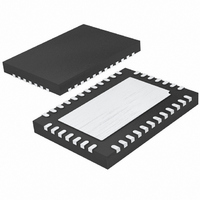
LT3513EUHF#TRPBF Linear Technology, LT3513EUHF#TRPBF Datasheet - Page 12

LT3513EUHF#TRPBF
Manufacturer Part Number
LT3513EUHF#TRPBF
Description
IC REG 5-OUT FOR TFT-LCD 38QFN
Manufacturer
Linear Technology
Datasheet
1.LT3513EUHFPBF.pdf
(22 pages)
Specifications of LT3513EUHF#TRPBF
Applications
Converter, TFT, LCD
Voltage - Input
4.5 ~ 30 V
Number Of Outputs
5
Voltage - Output
0.8 ~ 40 V
Operating Temperature
-40°C ~ 125°C
Mounting Type
Surface Mount
Package / Case
38-QFN
Lead Free Status / RoHS Status
Lead free / RoHS Compliant
Available stocks
Company
Part Number
Manufacturer
Quantity
Price
LT3513
operaTion
A power good comparator monitors AV
when FB2 is at or above 90% of its regulated value. The
output is an open-collector transistor that is off when the
output is out of regulation, allowing an external resistor
to pull the pin high. This pin can be used with a P-channel
MOSFET that functions as an output disconnect for AV
The four switchers are current mode regulators. Instead
of directly modulating the duty cycle of the power switch,
the feedback loop controls the peak current in the switch
during each cycle. Compared to voltage mode control, cur-
rent mode control improves loop dynamics and provides
cycle-by-cycle current limit.
All four switchers employ a constant-frequency current
mode control scheme. Switcher 1, the step-down regula-
tor, differs slightly from the others with inductor current
sense. Instead of monitoring the current at the switch,
current nodes are used to measure the current through
the inductor. Inductor current sense does not suffer from
minimum on-time problems, therefore always keep-
ing the switch current limited with any input-to-output
voltage ratio. Switcher 1 is always synchronized to the
master oscillator. The other three switchers each have
their own slave oscillator. The slave oscillator reduces the
frequency when the feedback voltage dips below 0.75V
and decreases linearly below the threshold as shown in
the Performance Characteristics’ Frequency Foldback plot.
Other than these two differences, the control loop is similar
in all four switchers. A pulse from the master oscillator
for switcher 1 or a pulse from the slave oscillator for the
other three switchers sets the RS latch and turns on the
internal NPN bipolar power switch. Current in the switch
and the external inductor begins to increase. When this
current exceeds a level determined by the voltage at V
current comparator resets the latch, turning off the switch.
The current in the inductor flows through the Schottky
12
DD
and turns on
C
, the
DD
.
diode and begins to decrease. The cycle begins again at
the next pulse from the oscillator. In this way, the voltage
on the V
the output. The internal error amplifier regulates the output
by continually adjusting the V
for switching on the V
of 1.8V limits the V
contain an independent current limit not dependent on V
or duty cycle. Switcher 1’s current limit is controlled by
the V
ers also use slope compensation to ensure stability with
the current mode scheme at duty cycles above 50%. The
RUN-SS1, RUN-SS2 and RUN-SS3/4 pins control the rate
of rise of the feedback pins.
The switch driver for SW1 operates either from V
the BOOST pin. An external capacitor and an integrated
Schottky diode are used to generate a voltage at the BOOST
pin that is higher than the input supply. This allows the
driver to saturate the internal bipolar NPN power switch
for efficient operation.
INPUT VOLTAGE RANGE STEP-DOWN CONSIDERATION
The minimum operating voltage of switcher 1 is determined
either by the LT3513’s undervoltage lockout of ~4V or by
its maximum duty cycle. A user defined undervoltage
lockout may be set with the UVLO pin at a voltage higher
than the internal undervoltage lockout. The duty cycle is
the fraction of time that the internal switch is on and is
determined by the input and output voltages:
where V
(~0.4V) and V
Dc =
C
voltage and varies with duty cycle. All four switch-
C
F
V
pin controls the current through the inductor to
IN
is the forward voltage drop of the catch diode
V
– V
OUT
SW
SW
+ V
is the voltage drop of the internal switch
+ V
C
F
voltage. Switchers 2, 3 and 4 also
F
C
pin is 0.8V, and an active clamp
C
pin voltage. The threshold
IN
or from
3513fc
C


