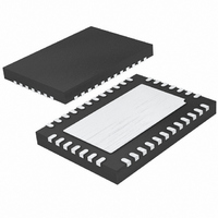
LT3513EUHF#TRPBF Linear Technology, LT3513EUHF#TRPBF Datasheet - Page 4

LT3513EUHF#TRPBF
Manufacturer Part Number
LT3513EUHF#TRPBF
Description
IC REG 5-OUT FOR TFT-LCD 38QFN
Manufacturer
Linear Technology
Datasheet
1.LT3513EUHFPBF.pdf
(22 pages)
Specifications of LT3513EUHF#TRPBF
Applications
Converter, TFT, LCD
Voltage - Input
4.5 ~ 30 V
Number Of Outputs
5
Voltage - Output
0.8 ~ 40 V
Operating Temperature
-40°C ~ 125°C
Mounting Type
Surface Mount
Package / Case
38-QFN
Lead Free Status / RoHS Status
Lead free / RoHS Compliant
Available stocks
Company
Part Number
Manufacturer
Quantity
Price
LT3513
elecTrical characTerisTics
temperature range, otherwise specifications are at T
PARAMETER
Switch 3 (250mA BOOST)
FB3 Voltage
FB3 Voltage Line Regulation
FB3 Pin Bias Current
Error Amplifier 3 Voltage Gain
Error Amplifier 3 Transconductance
Switch 3 Current Limit
Switch 3 V
Switch 3 Leakage Current
BIAS Pin Current Due to SW3
Maximum Duty Cycle (SW3)
Schottky Diode Drop
Switch 4 (250mA Inverter)
NFB4 Voltage
NFB4 Voltage Line Regulation
NFB4 Pin Bias Current
Error Amplifier 4 Voltage Gain
Error Amplifier 4 Transconductance
Switch 4 Current Limit
Switch 4 V
Switch 4 Leakage Current
BIAS Pin Current Due to SW4
Maximum Duty Cycle (SW4)
Schottky Diode Drop (D4)
NPN LDO
FB5 Voltage
FB5 Pin Bias Current
Base Drive Current
LDOPWR Minimum Voltage
Note 1: Stresses beyond those listed under Absolute Maximum Ratings
may cause permanent damage to the device. Exposure to any Absolute
Maximum Rating condition for extended periods may affect device
reliability and lifetime.
Note 2: The LT3513E is guaranteed to meet specified performance from
0°C to 125°C junction temperature. Specifications over the –40°C to
125°C operating junction temperature range are assured by design,
characterization and correlation with statistical process controls. The
LT3513I is guarenteed over the full –40°C to 125°C operating junction
temperature range.
Note 3: The C
above the FB threshold offset.
Note 4: Current flows out of FB1, FB3, NFB4 and FB5.
4
CESAT
CESAT
T
pin is held low until FB1, FB2, FB3 and NFB4 all ramp
CONDITIONS
4.5V < V
(Note 4)
ΔI = 10µA
(Note 6)
I
FB3 = 1.5V, RUN-SS1 = 0V
I
I = 170mA
4.5V < V
(Note 4)
ΔI = 10µA
(Note 6)
I
NFB4 = –1.5V, RUN-SS1 = 0V
I
I = 170mA
(Note 4)
FB5 = 0.5V
BD = 3.5V
SW3
SW3
SW4
SW4
= 0.2A
= 0.2A
= 0.2A
= 0.2A
IN
IN
A
< 30V
< 30V
= 25°C. V
The
l
IN
denotes the specifications which apply over the full operating
= 12V, BIAS = 3V, unless otherwise noted.
Note 5: Current may flow in or out of FB2. The absolute value of this test
is used.
Note 6: Current limit is guaranteed by design and/or correlation to static
test. Slope compensation reduces current limit at higher duty cycles.
Note 7: This is the minimum voltage across the boost capacitor needed to
guarantee full saturation of the internal power switch.
Note 8: This IC includes overtemperature protection that is intended
to protect the device during momentary overload conditions. Junction
temperature will exceed the maximum operating junction temperature
range when overtemperature protection is active. Continuous operation
above the specified maximum operating junction temperature may impair
device reliability.
l
l
l
l
l
l
l
–1.205
–1.215
1.20
1.19
0.25
0.25
0.61
MIN
0.6
4.5
84
84
6
–1.180
0.625
1.22
0.01
0.01
TYP
250
220
200
900
200
220
200
700
0.3
0.1
0.3
0.1
30
18
88
18
88
30
5
8
–1.155
–1.145
MAX
1.24
1.25
0.03
0.38
0.03
0.40
0.63
0.65
200
200
16
10
1
1
µmhos
µmhos
UNITS
3513fc
%/V
%/V
V/V
V/V
mV
mA
mV
mV
mA
mV
mA
nA
µA
µA
µA
nA
%
%
V
V
A
V
V
A
V
V
V


