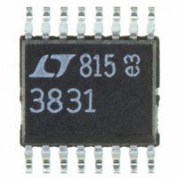
LTC3831EGN#PBF Linear Technology, LTC3831EGN#PBF Datasheet - Page 11

LTC3831EGN#PBF
Manufacturer Part Number
LTC3831EGN#PBF
Description
IC SW REG CONTROLLR SYNC 16-SSOP
Manufacturer
Linear Technology
Datasheet
1.LTC3831EGNTR.pdf
(20 pages)
Specifications of LTC3831EGN#PBF
Applications
Controller, DDR
Voltage - Input
3 ~ 8 V
Number Of Outputs
1
Voltage - Output
1.27 ~ 4 V
Operating Temperature
-40°C ~ 85°C
Mounting Type
Surface Mount
Package / Case
16-SSOP
Primary Input Voltage
8V
No. Of Outputs
1
Output Current
10A
No. Of Pins
16
Operating Temperature Range
-40°C To +85°C
Msl
MSL 1 - Unlimited
Supply Voltage Range
3V To 8V
Rohs Compliant
Yes
Lead Free Status / RoHS Status
Lead free / RoHS Compliant
Available stocks
Company
Part Number
Manufacturer
Quantity
Price
APPLICATIONS INFORMATION
controller feedback loop. As a result, the loop crossover
frequency increases and it may cause the feedback loop
to be unstable if the phase margin is insuffi cient.
To overcome this problem, the LTC3831 monitors the
peak voltage of the ramp signal and adjust the oscillator
charging current to maintain a constant ramp peak.
Input Supply Considerations/Charge Pump
The LTC3831 requires four supply voltages to operate: V
for the main power input, PV
gate drive and a clean, low ripple V
internal circuitry (Figure 5).
In many applications, V
through an RC fi lter. This supply can be as low as 3V. The
low quiescent current (typically 800μA) allows the use
of relatively large fi lter resistors and correspondingly
small fi lter capacitors. 100Ω and 4.7μF usually provide
adequate fi ltering for V
the 4.7μF bypass capacitor as close to the LTC3831 V
pin as possible.
Gate drive for the top N-channel MOSFET Q1 is supplied
from PV
SYNC METHOD
TERMINATION
UNDER SYNC
TRADITIONAL
KEEPS RAMP
WITH EARLY
AMPLITUDE
CONSTANT
LTC3831
RAMP
RAMP AMPLITUDE
CC1
Figure 4. External Synchronization Operation
SHDN
FREE RUNNING
ADJUSTED
. This supply must be above V
RAMP SIGNAL
200kHz
CC
. For best performance, connect
CC
can be powered from V
CC1
and PV
CC
IN
for the LTC3831
CC2
WITH EXT SYNC
(the main power
RAMP SIGNAL
for MOSFET
3831 F04
CC
IN
IN
supply input) by at least one power MOSFET V
effi cient operation. An internal level shifter allows PV
operate at voltages above V
This higher voltage can be supplied with a separate supply,
or it can be generated using a charge pump.
Gate drive for the bottom MOSFET Q2 is provided through
PV
V
from the same supply/charge pump for the PV
be connected to a lower supply to improve effi ciency.
Figure 6 shows a doubling charge pump circuit that can be
used to provide 2V
consists of a Schottky diode from V
capacitor from PV
Q2. This circuit provides 2V
ON and V
voltage of the Schottky diode. Ringing at the drain of Q2
can cause transients above 2V
GS(ON)
USE FOR V
LTC3831
CC2
OPTIONAL
D
12V
1N5242
Z
CIRCUITRY
INTERNAL
. This supply only need to be above the power MOSFET
V
CC
IN
for effi cient operation. PV
IN
≥ 7V
LTC3831
– V
PV
Figure 6. Doubling Charge Pump
F
CC2
PV
while Q1 is OFF where V
CC1
Figure 5. Supplies Input
CC2
IN
gate drive for Q1. The charge pump
PV
to the switching node at the drain of
CC1
PV
TG
BG
CC1
CC
IN
and V
MBR0530T1
0.1μF
IN
TG
BG
– V
at PV
IN
CC2
F
IN
V
IN
, up to 14V maximum.
to PV
V
Q1
Q2
to PV
IN
CC1
Q1
Q2
can also be driven
LTC3831
L
O
F
; if V
CC1
CC1
L
is the forward
O
CC1
+
while Q1 is
and a 0.1μF
IN
+
GS(ON)
3831 F05
, or it can
is higher
C
11
OUT
3831 F06a
C
V
CC1
OUT
OUT
V
3831fb
OUT
for
to


