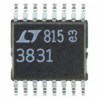
LTC3831EGN#PBF Linear Technology, LTC3831EGN#PBF Datasheet - Page 7

LTC3831EGN#PBF
Manufacturer Part Number
LTC3831EGN#PBF
Description
IC SW REG CONTROLLR SYNC 16-SSOP
Manufacturer
Linear Technology
Datasheet
1.LTC3831EGNTR.pdf
(20 pages)
Specifications of LTC3831EGN#PBF
Applications
Controller, DDR
Voltage - Input
3 ~ 8 V
Number Of Outputs
1
Voltage - Output
1.27 ~ 4 V
Operating Temperature
-40°C ~ 85°C
Mounting Type
Surface Mount
Package / Case
16-SSOP
Primary Input Voltage
8V
No. Of Outputs
1
Output Current
10A
No. Of Pins
16
Operating Temperature Range
-40°C To +85°C
Msl
MSL 1 - Unlimited
Supply Voltage Range
3V To 8V
Rohs Compliant
Yes
Lead Free Status / RoHS Status
Lead free / RoHS Compliant
Available stocks
Company
Part Number
Manufacturer
Quantity
Price
PIN FUNCTIONS
FREQSET (Pin 11): Frequency Set. Use this pin to adjust
the free-running frequency of the internal oscillator. With
the pin fl oating, the oscillator runs at about 200kHz. A
resistor from FREQSET to ground speeds up the oscillator;
a resistor to V
I
threshold for the internal current limit comparator. If I
drops below I
rent limit. I
Connect this pin to the main V
Q1, through an external resistor to set the current limit
threshold. Connect a 0.1μF decoupling capacitor across
this resistor to fi lter switching noise.
I
switching node at the source of Q1 and the drain of Q2
BLOCK DIAGRAM
MAX
FB
(Pin 13): Current Limit Sense. Connect this pin to the
(Pin 12): Current Limit Threshold Set. I
MAX
FREQSET
MAX
COMP
SHDN
CC
SS
has an internal 12μA pull-down to GND.
slows it down.
with TG on, the LTC3831 goes into cur-
Q
C
12μA
100μs DELAY
OSCILLATOR
INTERNAL
2.2V
1.2V
QSS
IN
V
+
REF
supply at the drain of
ERR
DISABLE
–
I
–
+
LIM
THERMAL SHUTDOWN
PWM
CC
LOGIC AND
MAX
V
REF
–
+
–
– 3%
sets the
MIN
POWER DOWN
+
12μA
FB
V
I
I
FB
MAX
REF
V
–
through a 1k resistor. The 1k resistor is required to prevent
voltage transients from damaging I
for sensing the voltage drop across the upper N-channel
MOSFET, Q1.
V
circuits draw their supply from this pin. This pin requires
a 4.7μF bypass capacitor to GND.
PV
pin to the main high power supply.
BG (Pin 16): Bottom Driver Output . Connect this pin to
the gate of the lower N-channel MOSFET, Q2. This output
swings from PGND to PV
or during shutdown mode. To prevent output undershoot
during a soft-start cycle, BG is held low until TG fi rst goes
high (FFBG in the Block Diagram).
+ 3%
DISABLE GATE DRIVE
CC
MAX
+
–
CC2
(Pin 14): Power Supply Input. All low power internal
+
PV
V
(Pin 15): Power Supply Input for BG. Connect this
CC1
POR
CC1
+ 2.5V
S
R
S
R
FFBG
Q
Q
Q
ENABLE
BG
V
V
CC2
REF
REF
+ 3%
– 3%
V
. It remains low when TG is high
REF
24k
750Ω
750Ω
24k
3830 BD
FB
.This pin is used
LTC3831
V
PV
TG
PV
BG
PGND
FB
R
R
GND
CC
+
–
CC1
CC2
3831fb
7


