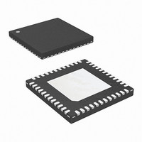
ISL6333AIRZ-T Intersil, ISL6333AIRZ-T Datasheet - Page 26

ISL6333AIRZ-T
Manufacturer Part Number
ISL6333AIRZ-T
Description
IC CTRLR PWM 3PHASE BUCK 48-QFN
Manufacturer
Intersil
Datasheet
1.ISL6333ACRZ.pdf
(40 pages)
Specifications of ISL6333AIRZ-T
Applications
Controller, Intel VR11
Voltage - Input
5 ~ 12 V
Number Of Outputs
1
Voltage - Output
0.5 ~ 1.6 V
Operating Temperature
-40°C ~ 85°C
Mounting Type
Surface Mount
Package / Case
48-VQFN
Lead Free Status / RoHS Status
Lead free / RoHS Compliant
Available stocks
Company
Part Number
Manufacturer
Quantity
Price
Compensating Dynamic VID Transitions
During a VID transition, the resulting change in voltage on the
FB pin and the COMP pin causes an AC current to flow through
the error amplifier compensation components from the FB to
the COMP pin. This current then flows through the feedback
resistor, R
undershoot at the end of the VID transition. In order to ensure
the smooth transition of the output voltage during a VID
change, a VID-on-the-fly compensation network is required.
This network is composed of a resistor and capacitor in series,
R
This VID-on-the-fly compensation network works by
sourcing AC current into the FB node to offset the effects of
the AC current flowing from the FB to the COMP pin during a
VID transition. To create this compensation current the
controllers set the voltage on the DVC pin to be 2x the
voltage on the REF pin. Since the error amplifier forces the
voltage on the FB pin and the REF pin to be equal, the
resulting voltage across the series RC between DVC and FB
is equal to the REF pin voltage. The RC compensation
components, R
create the desired amount of compensation current.
The amount of compensation current required is dependant on
the modulator gain of the system, K1, and the error amplifier R-
C components, R
and COMP pins. Use Equations 15, 16, and 17 to calculate the
RC component values, R
compensation network. For these equations: V
voltage for the power train; V
amplitude (1.5V); and R
components between the FB and COMP pins.
K1
R
C
DVC
DVC
DVC
FIGURE 10. DYNAMIC VID COMPENSATION NETWORK
=
C
REF
REF
---------- -
V
and C
V
=
=
PP
IN
VDIFF
A R
C
------- -
FB
A
C
×
DVC
, and can cause the output voltage to overshoot or
DVC
C
DVC
V
, between the DVC and the FB pin.
C
DAC
A
C
and C
DVC
=
and C
x2
---------------- -
K1 1
I
C
DVC
K1
DVC
R
C
and C
–
FB
, that are in series between the FB
DVC
P-P
R
26
and C
DVC
, can then be selected to
I
C
DVC
ISL6333 INTERNAL CIRCUIT
is the oscillator ramp
are the error amplifier R-C
DVC
= I
ISL6333, ISL6333A, ISL6333B, ISL6333C
FB
C
, for the VID-on-the-fly
C
C
+
-
AMPLIFIER
IN
I
ERROR
C
R
is the input
C
(EQ. 15)
(EQ. 16)
(EQ. 17)
COMP
Driver Operation
Adaptive Zero Shoot-Through Deadtime Control
The integrated drivers incorporate an adaptive deadtime control
technique to minimize deadtime and to prevent the upper and
lower MOSFETs from conducting simultaneously. This results
in high efficiency from the reduced freewheeling time of the
lower MOSFET body-diode conduction. This is accomplished
by ensuring either rising gate turns on its MOSFET with
minimum and sufficient delay after the other has turned off.
During turn-off of the lower MOSFET, the LGATE voltage is
monitored until it reaches 1.75V. At this time the UGATE is
released to rise. Once the PHASE is high, the advanced
adaptive shoot-through circuitry monitors the PHASE and
UGATE voltages during a PWM falling edge and the
subsequent UGATE turn-off. If either the UGATE falls to less
than 1.75V above the PHASE or the PHASE falls to less than
+0.8V, the LGATE is released to turn on.
Internal Bootstrap Device
All three integrated drivers feature an internal bootstrap
schottky diode. Simply adding an external capacitor across
the BOOT and PHASE pins completes the bootstrap circuit.
The bootstrap function is also designed to prevent the
bootstrap capacitor from overcharging due to the large
negative swing at the PHASE node. This reduces voltage
stress on the boot to phase pins.
The bootstrap capacitor should have a maximum voltage
rating that’s at least 30% above PVCC and its capacitance
value can be chosen from Equation 18:
where Q
at V
control MOSFETs. The ΔV
allowable droop in the rail of the upper gate drive.
C
Q
FIGURE 11. BOOTSTRAP CAPACITANCE vs BOOT RIPPLE
BOOT_CAP
GATE
GS1
1.6
1.4
1.2
1.0
0.8
0.6
0.4
0.2
0.0
=
G1
0.0
gate-source voltage and N
Q
---------------------------------- N
20nC
G1
is the amount of gate charge per upper MOSFET
≥
V
0.1
VOLTAGE
------------------------------------- -
ΔV
⋅
GS1
PVCC
BOOT_CAP
Q
0.2
GATE
50nC
Q
GATE
⋅
0.3
Q1
BOOT_CAP
= 100nC
ΔV
0.4
BOOT_CAP
0.5
Q1
0.6
term is defined as the
is the number of
(V)
0.7
0.8
October 8, 2010
0.9
(EQ. 18)
FN6520.3
1.0


