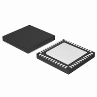
NCP4208MNR2G ON Semiconductor, NCP4208MNR2G Datasheet - Page 6

NCP4208MNR2G
Manufacturer Part Number
NCP4208MNR2G
Description
IC CTLR 8PH VR11.1 PMBUS 48-QFN
Manufacturer
ON Semiconductor
Datasheet
1.NCP4208MNR2G.pdf
(30 pages)
Specifications of NCP4208MNR2G
Applications
Controller, Intel VR11.1
Voltage - Input
4.7 ~ 5.75 V
Number Of Outputs
8
Voltage - Output
0.16 ~ 5 V
Operating Temperature
0°C ~ 85°C
Mounting Type
Surface Mount
Package / Case
48-TQFN Exposed Pad
Output Voltage
0.375 V to 1.6 V
Input Voltage
0.3 V to 6 V
Switching Frequency
1.5 MHz
Operating Temperature Range
0 C to + 85 C
Mounting Style
SMD/SMT
Duty Cycle (max)
100 %
Lead Free Status / RoHS Status
Lead free / RoHS Compliant
Available stocks
Company
Part Number
Manufacturer
Quantity
Price
Company:
Part Number:
NCP4208MNR2G
Manufacturer:
ON Semiconductor
Quantity:
1 200
Part Number:
NCP4208MNR2G
Manufacturer:
ON/安森美
Quantity:
20 000
ELECTRICAL CHARACTERISTICS
V
Reference Current
Error Amplifier
VID Inputs
Oscillator
Current Sense Amplifier
1. Performance guaranteed over the indicated operating temperature range by design and/or characterization tested at T
2. Refer to Application Information section.
3. Values based on design and/or characterization.
Reference Bias Voltage
Reference Bias Current
Output Voltage Range
Accuracy
Load Line Positioning Accuracy
Load Line Range
Load Line Attenuation
Differential Non−linearity
Input Bias Current
Offset Accuracy
FBRTN Current
Output Current
Gain Bandwidth Product
Slew Rate
BOOT Voltage Hold Time
Input Low Voltage
Input High Voltage
Input Current
VID Transition Delay Time
No CPU Detection Turn−Off Delay
Time
Frequency Range
Frequency Variation
Output Voltage
RAMPADJ Output Voltage
RAMPADJ Input Current Range
Offset Voltage
Input Bias Current, CSREF
Input Bias Current, CSSUM
Gain Bandwidth Product
Slew Rate
Input Common−Mode Range
Output Voltage Range
Output Current
Current Limit Latchoff Delay Time
IN
duty cycle pulse techniques are used during testing to maintain the junction temperature as close to ambient as possible.
= (5.0 V) FBRTN − GND, for typical values T
Parameter
R
Relative to nominal DAC output, referenced
to FBRTN (refer to Figure 4)
In startup
I
VR Offset Register = 111111, VID = 1.0 V
VR Offset Register = 011111, VID = 1.0 V
FB forced to V
COMP = FB
COMP = FB
Internal Timer
VID(X)
VID code change to FB change
VID code change to PWM going low
T
T
T
RT = 500 kW to GND
RAMPADJ − FB, V
IRAMPADJ = −150 mA
CSSUM − CSREF (refer to Figure 5)
CSREF = 1.0 V
CSREF = 1.0 V
CSSUM = CSCOMP
C
CSSUM and CSREF
Internal Timer
FB
A
A
A
IREF
CSCOMP
= 25°C, R
= 25°C, R
= 25°C, R
= I
IREF
= 121 kW
A
= 10 pF
= 25°C, for min/max values T
T
T
T
Test Conditions
OUT
= 500 kW, 4−phase
= 250 kW, 4−phase
= 121 kW, 4−phase
FB
http://onsemi.com
−3%
= 1.0 V,
6
A
= 0°C to 85°C; unless otherwise noted. (Notes 1 and 2)
I
I
BIAS(CSREF)
BIAS(CSSUM)
GBW
GBW
V
V
I
V
I
Symbol
RAMPADJ
V
V
CSCOMP
V
FB(BOOT)
RAMPADJ
I
I
f
I
OS(CSA)
V
t
FBRTN
IN(VID)
PHASE
I
COMP
IH(VID)
BOOT
IL(VID)
f
COMP
V
V
IREF
OSC
I
IREF
FB
FB
RT
(ERR)
(CSA)
1.091
−350
1.75
−9.0
−1.0
13.3
0.25
−1.0
0.05
Min
−77
400
170
−50
−20
−10
0.8
5.0
1.9
5.0
0
0
0
−193.75
193.75
−5.0
2.01
Typ
−80
100
500
195
375
750
500
1.8
1.1
2.0
8.0
15
15
20
25
10
10
J
= T
1.109
Max
1.85
+9.0
+1.0
18.5
+1.0
A
−83
100
200
225
+50
+20
+10
4.4
0.3
9.0
2.1
3.0
3.0
60
0
= 25_C. Low
MHz
MHz
MHz
Unit
LSB
V/ms
V/ms
kHz
mV
mV
mV
mV
mV
mV
ms
ms
mA
mA
mA
mA
mA
mA
mA
nA
mA
ns
ms
%
V
V
V
V
V
V
V


