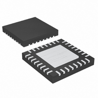
MAX1584ETJ+T Maxim Integrated Products, MAX1584ETJ+T Datasheet - Page 11

MAX1584ETJ+T
Manufacturer Part Number
MAX1584ETJ+T
Description
IC DGTL CAM PWR-SUP 5CH 32TQFN
Manufacturer
Maxim Integrated Products
Datasheet
1.MAX1585ETJ.pdf
(29 pages)
Specifications of MAX1584ETJ+T
Applications
Controller, Digital Camera
Voltage - Input
0.7 ~ 5.5 V
Number Of Outputs
5
Voltage - Output
1.25 ~ 5.5 V
Operating Temperature
-40°C ~ 85°C
Mounting Type
Surface Mount
Package / Case
32-TQFN Exposed Pad
Lead Free Status / RoHS Status
Lead free / RoHS Compliant
PIN
16
17
18
19
20
21
22
23
24
25
26
27
AUX1OK
NAME
SDOK
PGSU
INDL2
LXSU
PVSU
OSC
SCF
CC2
FB2
DL2
PV
______________________________________________________________________________________
Open-Drain Power-OK Signal for AUX1 Controller. AUX1OK is low when the AUX1 controller has
successfully completed soft-start. This pin is high impedance in shutdown, overload, and thermal limit.
Open-Drain Power-OK Signal for Step-Down Converter. SDOK is low when the step-down has successfully
completed soft-start. This pin is high impedance in shutdown, overload, and thermal limit.
Short-Circuit Flag, Active-Low, Open-Drain Output. SCF is high impedance when overload protection
occurs and during startup. SCF can drive high-side PFET switches connected to one or more outputs to
completely disconnect the load when the channel turns off in response to a logic command or an
overload. See the Status Outputs ( SDOK , AUX1OK , SCF) section.
Oscillator Control. Connect a timing capacitor from OSC to GND and a timing resistor from OSC to PVSU
(or other DC voltage) to set the oscillator frequency between 100kHz and 1MHz. See the Setting the
Switching Frequency section. This pin is high impedance in shutdown.
Step-Up Power Ground. Connect all PG_ pins together and to GND with short traces as close to the IC as
possible.
Step-Up Converter Switching Node. Connect to the inductor of the step-up converter. LXSU is high
impedance in shutdown.
Power Output of the Step-Up DC-DC Converter. Connect the output filter capacitor from PVSU to PGSU.
PVSU can also power other converter channels. Connect PVSU to PV at the IC.
AUX2 Controller Feedback Input.
This pin is high impedance in
shutdown.
AUX2 Controller Compensation Node. Connect a series resistor-capacitor from CC2 to GND to
compensate the control loop. CC2 is actively driven to GND in shutdown and thermal limit. See the AUX
Compensation section.
Voltage Input for the AUX2 Gate
Driver. The voltage at INDL2 sets
the high gate-drive voltage.
IC Power Input. Connect PVSU and PV together.
AUX2 Controller Gate-Drive
Output. DL2 drives between
INDL2 and GND.
5-Channel Slim DSC Power Supplies
MAX1585 (AUX2 inverter): The FB2 feedback threshold is 0V.
Connect a resistive voltage-divider from the output voltage to FB2 to
REF to set the output voltage.
MAX1584 (AUX2 step-up): The FB2 feedback threshold is 1.25V.
Connect a resistive voltage-divider from the output voltage to FB2 to
GND to set the output voltage.
MAX1585 (AUX2 inverter): Connect INDL2 to the external P channel
MOSFET source (typically the battery) to ensure the P channel is
completely off when D2 swings high.
MAX1584 (AUX2 step-up): Connect INDL2 to PVSU for optimum
N-channel gate drive.
MAX1585: DL2 drives a PFET in an inverter configuration. In
shutdown, overload, and thermal limit, DL2 is driven high.
MAX1584: DL2 drives an N-channel FET in a boost/flyback
configuration. In shutdown, overload, and thermal limit, DL2 is driven
low.
FUNCTION
Pin Description (continued)
11


