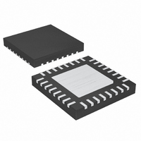
MAX1584ETJ+T Maxim Integrated Products, MAX1584ETJ+T Datasheet - Page 2

MAX1584ETJ+T
Manufacturer Part Number
MAX1584ETJ+T
Description
IC DGTL CAM PWR-SUP 5CH 32TQFN
Manufacturer
Maxim Integrated Products
Datasheet
1.MAX1585ETJ.pdf
(29 pages)
Specifications of MAX1584ETJ+T
Applications
Controller, Digital Camera
Voltage - Input
0.7 ~ 5.5 V
Number Of Outputs
5
Voltage - Output
1.25 ~ 5.5 V
Operating Temperature
-40°C ~ 85°C
Mounting Type
Surface Mount
Package / Case
32-TQFN Exposed Pad
Lead Free Status / RoHS Status
Lead free / RoHS Compliant
ABSOLUTE MAXIMUM RATINGS
PV, PVSU, PVSD,
GND..........................................................................-0.3V to +6V
PGND to GND....................................................…-0.3V to +0.3V
INDL2, DL1, DL3 to GND.........................-0.3V to (PVSU + 0.3V)
DL2 to GND ............................................-0.3V to (INDL2 + 0.3V)
PV to PVSU ...........................................................-0.3V to + 0.3V
LXSU Current (Note 1) ..........................................................3.6A
LXSD Current (Note 1) ........................................................2.25A
REF, OSC, CC_ to GND...........................-0.3V to (PVSU + 0.3V)
5-Channel Slim DSC Power Supplies
ELECTRICAL CHARACTERISTICS
(V
Note 1: LXSU has internal clamp diodes to PVSU and PGND, and LXSD has internal clamp diodes to PVSD and PGND. Applications
Stresses beyond those listed under “Absolute Maximum Ratings” may cause permanent damage to the device. These are stress ratings only, and functional
operation of the device at these or any other conditions beyond those indicated in the operational sections of the specifications is not implied. Exposure to
absolute maximum rating conditions for extended periods may affect device reliability.
2
GENERAL
Input Voltage Range
Step-Up Minimum Startup
Voltage
Shutdown Supply Current into PV
Supply Current into PV with
Step-Up Enabled
Supply Current into PV with
Step-Up and Step-Down Enabled
Total Supply Current from PV and
PVSU with Step-Up and One AUX
Enabled
REFERENCE
Reference Output Voltage
Reference Load Regulation
Reference Line Regulation
OSCILLATOR
OSC Discharge Trip Level
OSC Discharge Resistance
OSC Discharge Pulse Width
OSC Frequency
STEP-UP DC-DC CONVERTER
Step-Up Startup-to-Normal
Operating Threshold
Step-Up Startup-to-Normal
Operating Threshold Hysteresis
PVSU
_______________________________________________________________________________________
= V
that forward bias these diodes should take care not to exceed the device’s power dissipation limits.
PARAMETER
PV
= V
PVSD
SDOK, AUX1OK, SCF, ON_, FB_ to
= V
INDL2
= 3.6V, T
(Note 2)
I
-2300ppm/°C (typ) (Note 3)
PV = 3.6V
ONSU = 3.6V, FBSU = 1.5V
(does not include switching losses)
ONSU = ONSD = 3.6V, FBSU = 1.5V, FBSD = 1.5V
(does not include switching losses)
ONSU = ON1 = 3.6V, FBSU = 1.5V, FB2 = 1.5V
(does not include switching losses)
I
10µA < I
2.7 < PVSU < 5.5V
Rising edge
OSC = 1.5V, I
R
Rising edge or falling edge (Note 4)
LOAD
REF
OSC
= 20µA
A
= 47kΩ, C
< 1mA, T
= 0°C to +85°C, unless otherwise noted.)
REF
< 200µA
OSC
A
OSC
= +25°C, startup voltage tempco is
= 3mA
=100pF
CONDITIONS
Continuous Power Dissipation (T
Operating Temperature Range ...........................-40°C to +85°C
Junction Temperature ......................................................+150°C
Storage Temperature Range .............................-65°C to +150°C
Lead Temperature (soldering, 10s) .................................+300°C
32-Pin Thin QFN (derate 22mW/°C above +70°C) ....1700mW
1.225
MIN
1.23
2.30
0.7
A
= +70°C)
TYP
1.25
1.25
300
450
400
150
500
0.9
0.1
4.5
1.3
2.5
52
80
1.275
MAX
1.27
2.65
450
700
650
5.5
1.1
10
80
5
5
UNITS
kHz
mV
mV
mV
µA
µA
µA
µA
ns
Ω
V
V
V
V
V


