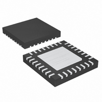
MAX1997ETJ+T Maxim Integrated Products, MAX1997ETJ+T Datasheet - Page 25

MAX1997ETJ+T
Manufacturer Part Number
MAX1997ETJ+T
Description
IC PWR SUPPLY TFT LCD 32TQFN
Manufacturer
Maxim Integrated Products
Datasheet
1.MAX1997ETJ.pdf
(31 pages)
Specifications of MAX1997ETJ+T
Applications
Controller, TFT, LCD
Voltage - Input
2.7 ~ 5.5 V
Number Of Outputs
5
Voltage - Output
2.7 ~ 13 V
Operating Temperature
0°C ~ 85°C
Mounting Type
Surface Mount
Package / Case
32-TQFN Exposed Pad
Lead Free Status / RoHS Status
Lead free / RoHS Compliant
After including the effects of resistor tolerance, com-
parator offset, and input voltage variation, the minimum
input overcurrent threshold equation is:
where V
input voltage, ε is the tolerance of the resistors, and 5mV
is the worst-case input offset voltage of the comparator.
To simplify the equation, define a constant (k) as follows:
The minimum threshold equation becomes:
Solving for R4/R5 yields:
The R4/R5 ratio guarantees the required minimum level
for I
The following example shows how to apply the above
equations in the design. If 1% resistors are used, then
ε = 0.01. To set V
R2 = 51.1kΩ and R3 = 150kΩ. Assume that the mini-
mum input voltage is 2.7V and the typical input voltage
is 3.3V, the average inductor current at maximum load
is 1.25A, and the maximum R
Quintuple/Triple-Output TFT LCD Power Supplies
R4
R5
L(MAX)
R4
R5
=
=
I
I
V
L(MAX)
TH_TYP
0 9802
IN(MIN)
0 2637
.
.
IN(MIN)
= ×
. The typical overcurrent threshold is given by:
5
V
k
IN(MIN)
mV
×
=
×
×
=
V
V
R
2.7V
is the minimum expected value of the
IN(MIN)
k
(
IN(MIN)
R
V
V
DS(TYP)
IN(TYP)
OCP
IN(MIN)
DS(MAX)
______________________________________________________________________________________
×
×
k =
×
R
R
R
2
R
150
4
1 + 0.01
2
1 - 0.01
to be around 75% of V
k =
with Fault Protection and VCOM Buffer
3
R
- I
×
×
+
Ω
2.7V - 1.25A 0.1
- I
3
)
(
1
1
L(MAX)
×
(
1
1
+
R
L(MAX)
+
+
+
R
R
×
+
+
0 9802 51 1
3
DS(ON)
3
5
ε
ε
R
1
.
150
ε
ε
k
R
)
3
)
-
+
=
×
×
4
+
×
+
Ω
0 9802
R3
R5
(
(
k
5
×
.
1
1
+
×
R
R
mV
×
R
+
+
×
of P1 is 100mΩ:
×
R
2
3
5
k
ε
ε
×
×
R
DS(MAX)
)
)
.
R
×
=
×
+
×
DS(MAX)
Ω
k
(R4 +R5)
(R2+R3)
5
(
Ω
(
(
V
5
1
1
R
IN(MIN)
mV
+
+
+
5
0 005
ε
ε
.
IN
)
)
+
, select
)
-
V
×
-
1
-
1
If R5 =150kΩ, then R4 = 39.2kΩ. The typical overcur-
rent threshold is:
For highest efficiency, always choose the lowest num-
ber of charge-pump stages that meet the output
requirement. The number of positive charge-pump
stages is given by:
where N
stages, V
output, V
is the forward voltage drop of the charge-pump diode,
and V
ulator. Use V
The number of negative charge-pump stages is given by:
where N
stages, V
output, V
is the forward-voltage drop of the charge-pump diode,
and V
ulator. Use V
The above equations are derived based on the
assumption that the first stage of the positive charge
pump is connected to V
negative charge pump is connected to ground.
Sometimes fractional stages are more desirable for bet-
ter efficiency. This can be done by connecting the first
stage to V
charge-pump stage is powered from V
above equations become:
I
TH_TYP
DROPOUT
DROPOUT
Selecting the Number of Charge-Pump Stages
=
NEG
N
POS
N
N
MAIN
MAIN
G_OFF
G_ON
POS
POS
NEG
0.047
IN
N
3.3V
DROPOUT
DROPOUT
NEG
is the number of positive charge-pump
is the number of negative charge-pump
or another available supply. If the first
=
is the main step-up regulator output, V
is the main step-up regulator output, V
=
=
is the positive linear-regulator (REG P)
Ω
is the dropout margin for the linear reg-
is the dropout margin for the linear reg-
is the negative linear-regulator (REG N)
V
V
- V
=
G_ON
G_ON
×
G_O FF
- V
1
G_O FF
-
V
= 2V.
= 2V.
1
150
MAIN
V
V
V
+ V
+ V
50
MAIN
MAIN
MAIN
MAIN
+ V
Ω
Ω
DROPOUT
DROPOUT
+ V
-
DROPOUT
×
×
2
-
-
-
(39.2k +1
(51.1k +1
and the first stage of the
2
2
2
DROPOUT
×
×
×
×
V
D
V
V
V
D
D
D
Ω
Ω
- V
- V
Charge Pumps
+ V
MAIN
IN
50
50
IN
IN
Ω
Ω
)
)
, then the
=
4 15
.
A
25
D
D


