AN8049SH-E1 Panasonic - SSG, AN8049SH-E1 Datasheet - Page 8
AN8049SH-E1
Manufacturer Part Number
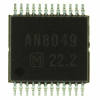
AN8049SH-E1
Description
IC MULTI CONFIG 40MA SSOP24D
Manufacturer
Panasonic - SSG
Type
Step-Down (Buck), Step-Up (Boost), Invertingr
Specifications of AN8049SH-E1
Internal Switch(s)
Yes
Synchronous Rectifier
No
Number Of Outputs
3
Current - Output
40mA
Frequency - Switching
20kHz ~ 1MHz
Voltage - Input
1.8 ~ 14 V
Operating Temperature
-30°C ~ 85°C
Mounting Type
Surface Mount
Package / Case
24-SSOP
Power - Output
146mW
Lead Free Status / RoHS Status
Contains lead / RoHS non-compliant
Voltage - Output
-
Other names
AN8049SHE1
AN8049SHE1TR
AN8049SHE1TR
Available stocks
Company
Part Number
Manufacturer
Quantity
Price
Company:

Part Number:
AN8049SH-E1V
Manufacturer:
MITSUMI
Quantity:
2 511
Part Number:
AN8049SH-E1V
Manufacturer:
PANASONIC/松下
Quantity:
20 000


AN8049SH
I Terminal Equivalent Circuits (continued)
8
Pin No.
10
11
7
8
9
16
16
20 kΩ
8
100 kΩ
7
10
11
1.1 µA
200 Ω
200 Ω
Equivalent circuit
1.26 V
V
I
I
SI(OUT)2
SI(OUT)1
CC
Start and stop of
internal circuits.
9
V
High
Channel 1
output operation
CC
I
I
SO(OUT)2
SO(OUT)1
30 kΩ
30 kΩ
13
12
SDH00012BEB
CTL1:
Controls the on/off state of channel 1. A delay
can be provided in the power supply turn-on start
time by connecting a capacitor between this pin
and ground.
(See the "Application Notes, [9]" section.)
t
This pin can also be used to control the on/off
state with an external signal. In that case, the
allowable input voltage range is from 0 V to V
Note that during U.V.L.O. and timer latch
operation, this pin is connected to ground through
a 20 kΩ resistor.
Off:
Controls the on/off state.
When the input is high: normal operation
(V
When the input is low: standby mode
(V
In standby mode, the total current consumption
is held to under 1 µA.
V
Outputs the internal reference voltage.
The reference voltage is 1.26 V (allowance:
±1%) when V
Insert a capacitor of at least 0.1 µF between V
and ground for phase compensation.
RB2:
Connection for a resistor that sets the channel 2
output current.
Use a resistor in the range 750 Ω to 15 kΩ.
RB1:
Connection for a resistor that sets the channel 1
output current.
Use a resistor in the range 750 Ω to 15 kΩ.
DLY3
REF
OFF
OFF
:
= 1.26 (V) × C
> 1.2 V)
< 0.6 V)
CC
is 2.4 V and I
Description
CTL1
(µF)/1.1 (µA) (s)
REF
is − 0.1 mA.
REF
CC
.
I/O
O
I
I
I
I
Related parts for AN8049SH-E1
Image
Part Number
Description
Manufacturer
Datasheet
Request
R

Part Number:
Description:
IC CIRCUIT PROTECTOR 1A SMINI 2P
Manufacturer:
Panasonic - SSG
Datasheet:
Part Number:
Description:
IC CIRCUIT PROTECTR .7A SMINI 2P
Manufacturer:
Panasonic - SSG
Datasheet:

Part Number:
Description:
IC CIRCUIT PROTCTR 1.2A SMINI 2P
Manufacturer:
Panasonic - SSG
Datasheet:

Part Number:
Description:
IC CIRCUIT PROTECTR 1.2A SNMP 2P
Manufacturer:
Panasonic - SSG
Datasheet:
Part Number:
Description:
IC CIRCUIT PROTECTOR 1A SNMP 2P
Manufacturer:
Panasonic - SSG
Datasheet:
Part Number:
Description:
IC CIRCUIT PROTECTR 1.8A SNMP 2P
Manufacturer:
Panasonic - SSG
Datasheet:
Part Number:
Description:
IC CIRCUIT PROTECTR 2.3A SNMP 2P
Manufacturer:
Panasonic - SSG
Datasheet:

Part Number:
Description:
DIODE ZENER DUAL 6.2V SSMINI-3
Manufacturer:
Panasonic - SSG
Datasheet:
Part Number:
Description:
DIODE ZENER DUAL 6.8V SSSMINI3P
Manufacturer:
Panasonic - SSG
Datasheet:

Part Number:
Description:
DIODE ZENER QUAD 12V SSMINI-5
Manufacturer:
Panasonic - SSG
Datasheet:
Part Number:
Description:
DIODE ZENER 15V 150MW S-MINI 2P
Manufacturer:
Panasonic - SSG
Datasheet:


Part Number:
Description:
DIODE ZENER 9.1V 150MW SSMINI-2
Manufacturer:
Panasonic - SSG
Datasheet:
Part Number:
Description:
DIODE ZENER 15V 150MW SSMINI-2
Manufacturer:
Panasonic - SSG
Datasheet: