LTC3535EDD#PBF Linear Technology, LTC3535EDD#PBF Datasheet
LTC3535EDD#PBF
Specifications of LTC3535EDD#PBF
Available stocks


Related parts for LTC3535EDD#PBF


LTC3535EDD#PBF Summary of contents
Page 1
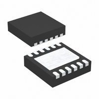
... The LTC3535 is housed in a 3mm × 3mm × 0.75mm DFN package. L, LT, LTC, LTM, Linear Technology, Burst Mode and the Linear logo are registered trademarks of Linear Technology Corporation. All other trademarks are the property of their respective owners. V ...
Page 2
... Storage Temperature Range ................... –65°C to 150°C ORDER INFORMATION LEAD FREE FINISH TAPE AND REEL LTC3535EDD#PBF LTC3535EDD#TRPBF Consult LTC Marketing for parts specified with wider operating temperature ranges. Consult LTC Marketing for information on non-standard lead based finish parts. For more information on lead free part marking, go to: ...
Page 3
ELECTRICAL CHARACTERISTICS operating temperature range of –40°C to 85°C, otherwise specifications are at T PARAMETER Minimum Duty Cycle Switching Frequency SHDN Pin Input High Voltage SHDN Pin Input Low Voltage Note 1: Stresses beyond those listed under Absolute Maximum Ratings ...
Page 4
LTC3535 TYPICAL PERFORMANCE CHARACTERISTICS Efficiency vs Load Current and V for OUT 100 EFFICIENCY POWER LOSS 1. 2. 3.6V IN ...
Page 5
TYPICAL PERFORMANCE CHARACTERISTICS DS(ON) OUT 0.90 0.85 0.80 0.75 0.70 0.65 PMOS 0.60 0.55 0.50 0.45 NMOS 0.40 0.35 0.30 1.5 2.0 2.5 3.0 3.5 4.0 4.5 V (V) OUT 3535 G10 V vs Temperature FB 0.50 ...
Page 6
LTC3535 TYPICAL PERFORMANCE CHARACTERISTICS Load Step Response (from Burst Mode Operation) V OUT 100mV/DIV AC-COUPLED LOAD CURRENT 50mA/DIV V = 3.6V 100µs/DIV OUT 20mA TO 170mA STEP C = 10µF OUT Load Step Response (Fixed Frequency) ...
Page 7
PIN FUNCTIONS V (Pin 1): Output Voltage Sense and Drain of the OUT1 Internal Synchronous Rectifier for Channel 1. PCB trace length from V to the output filter capacitor (4.7µF OUT1 minimum) should be as short and wide as possible. ...
Page 8
LTC3535 BLOCK DIAGRAM V IN1 0. 2.2µF SHDN1 11 SHUTDOWN 4M V REF UVLO START-UP THERMAL SHUTDOWN L2 4.7µH SW2 5 V IN2 V IN2 0. IN2 2.2µF SHDN2 8 SHUTDOWN 4M ...
Page 9
OPERATION (Refer to Block Diagram) The LTC3535 is a dual channel 1MHz synchronous boost converter housed in a 12-lead 3mm × 3mm DFN package. Each channel is identical and fully independent. They can operate from the same source, or from ...
Page 10
LTC3535 OPERATION (Refer to Block Diagram) the test mode being engaged. Refer to Figure 1 for two possible implementations. LTC3535 ±30% SHDN R V CNTRL 1M R > 0.4) – 1)M CNTRL IN Figure ...
Page 11
OPERATION (Refer to Block Diagram) Burst Mode OPERATION Each channel of the LTC3535 will enter Burst Mode operation at light load current and return to fixed frequency PWM mode when the load increases. Refer to the Typical Performance Characteristics to ...
Page 12
LTC3535 APPLICATIONS INFORMATION COMPONENT SELECTION Inductor Selection The LTC3535 can utilize small surface mount chip induc- tors due to their fast 1MHz switching frequency. Inductor values between 3.3µH and 6.8µH are suitable for most applications. Larger values of inductance will ...
Page 13
APPLICATIONS INFORMATION 4.7µF to 10µF output capacitor is sufficient for most ap- plications. Larger values may be used to obtain extremely low output voltage ripple and improve transient response. X5R and X7R dielectric materials are preferred for their ability to ...
Page 14
LTC3535 PACKAGE DESCRIPTION 3.50 ± 0.05 2.10 ± 0.05 1.65 ± 0.05 0.25 ± 0.05 RECOMMENDED SOLDER PAD PITCH AND DIMENSIONS APPLY SOLDER MASK TO AREAS THAT ARE NOT SOLDERED PIN 1 TOP MARK (SEE NOTE 6) 0.200 REF NOTE: ...
Page 15
... Added new Typical Application and Updated Related Parts table Information furnished by Linear Technology Corporation is believed to be accurate and reliable. However, no responsibility is assumed for its use. Linear Technology Corporation makes no representa- tion that the interconnection of its circuits as described herein will not infringe on existing patent rights. ...
Page 16
... V = 5.25V 9µA, IN OUT(MAX 0. 5.25V 12µA, IN OUT(MAX 0. 5.25V 12µA, IN OUT(MAX 0. 5.25V 30µA, IN OUT(MAX 0. 5.25V 10µA, IN OUT(MAX 0910 REV A • PRINTED IN USA LINEAR TECHNOLOGY CORPORA TION 2009 V OUT 1.78M 30.1k 1M 3535 TA03 3535fa ...