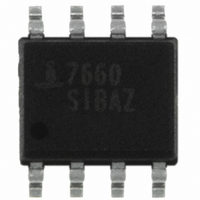
ICL7660SIBAZT Intersil, ICL7660SIBAZT Datasheet - Page 7

ICL7660SIBAZT
Manufacturer Part Number
ICL7660SIBAZT
Description
IC VOLTAGE CONVERTER CMOS 8-SOIC
Manufacturer
Intersil
Type
Switched Capacitor (Charge Pump), Doubler, Invertingr
Datasheet
1.ICL7660SIBAZT.pdf
(12 pages)
Specifications of ICL7660SIBAZT
Internal Switch(s)
Yes
Synchronous Rectifier
No
Number Of Outputs
1
Frequency - Switching
10kHz, 35kHz
Voltage - Input
1.5 ~ 12 V
Operating Temperature
-40°C ~ 85°C
Mounting Type
Surface Mount
Package / Case
8-SOIC (3.9mm Width)
Rohs Compliant
YES
Peak Reflow Compatible (260 C)
Yes
Lead Free Status / RoHS Status
Lead free / RoHS Compliant
Current - Output
-
Voltage - Output
-
Power - Output
-
Other names
ICL7660SIBAZTTR
Available stocks
Company
Part Number
Manufacturer
Quantity
Price
Company:
Part Number:
ICL7660SIBAZT
Manufacturer:
Intersil
Quantity:
301
Part Number:
ICL7660SIBAZT
Manufacturer:
RENESAS/瑞萨
Quantity:
20 000
The ICL7660S approaches these conditions for negative
voltage conversion if large values of C
ENERGY IS LOST ONLY IN THE TRANSFER OF CHARGE
BETWEEN CAPACITORS IF A CHANGE IN VOLTAGE
OCCURS. The energy lost is defined by:
where V
and transfer cycles. If the impedances of C
relatively high at the pump frequency (refer to Figure 13)
compared to the value of R
difference in the voltages V
desirable to make C
voltage ripple, but also to employ a correspondingly large
value for C
operation.
Do’s and Don’ts
E
V
1. Do not exceed maximum supply voltages.
2. Do not connect LV terminal to GND for supply voltage
3. Do not short circuit the output to V
4. When using polarized capacitors, the + terminal of C
5. If the voltage supply driving the ICL7660S has a large
6. User should insure that the output (pin 5) does not go
IN
FIGURE 13. IDEALIZED NEGATIVE VOLTAGE CONVERTER
=
8
greater than 3.5V.
voltages above 5.5V for extended periods, however,
transient conditions including start-up are okay.
must be connected to pin 2 of the ICL7660S and the +
terminal of C
source impedance (25Ω to 30Ω), then a 2.2μF capacitor
from pin 8 to ground may be required to limit rate of rise
of input voltage to less than 2V/µs.
more positive than GND (pin 3). Device latch up will occur
under these conditions. A 1N914 or similar diode placed
in parallel with C
under these conditions. (Anode pin 5, Cathode pin 3).
1
-- - C
2
3
1
1
(
V
and V
1
1
2
in order to achieve maximum efficiency of
–
S
S
V
3
1
2
2
2
7
are the voltages on C
2
must be connected to GND.
)
2
2
as large as possible to eliminate output
will prevent the device from latching up
2
4
L
1
, there will be substantial
and V
C
7
1
S
S
4
2
2
. Therefore it is not only
+
1
1
and C
supply for supply
during the pump
1
and C
2
are used.
C
2
V
2
OUT
are
3
5
(EQ. 1)
= -V
1
ICL7660S
IN
Typical Applications
Simple Negative Voltage Converter
The majority of applications will undoubtedly utilize the
ICL7660S for generation of negative supply voltages.
Figure 14 shows typical connections to provide a negative
supply where a positive supply of +1.5V to +12V is available.
Keep in mind that pin 6 (LV) is tied to the supply negative
(GND) for supply voltage below 3.5V.
The output characteristics of the circuit in Figure 14 can be
approximated by an ideal voltage source in series with a
resistance as shown in Figure 14B. The voltage source has
a value of -(V+). The output impedance (R
the ON resistance of the internal MOS switches (shown in
Figure 13), the switching frequency, the value of C
and the ESR (equivalent series resistance) of C
good first order approximation for R
R
f
Combining the four R
R
voltage and temperature (See the Output Source Resistance
graphs), typically 23Ω at +25°C and 5V. Careful selection of
C
output impedance. High value capacitors will reduce the
1/(f
the ESR term. Increasing the oscillator frequency will reduce
the 1/(f
increase in output impedance when C
enough to fully charge the capacitors every cycle. In a typical
application where f
------------------------------- -
f
10µF
R
PUMP
PUMP
0
FIGURE 14. SIMPLE NEGATIVE CONVERTER AND ITS
SW
1
0
≅
PUMP
and C
+
≅
-
2 R
, the total switch resistance, is a function of supply
1
2xR
(
(
×
PUMP
=
C
SW1
SW
2
f
------------- -
x C
1
2
3
4
1
OSC
will reduce the remaining terms, minimizing the
2
+
+
1
ESR
x C
OUTPUT EQUIVALENT
+
) component, and low ESR capacitors will lower
ICL7660S
------------------------------- -
f
PUMP
R
(
R
1
SW3
C2
) term, but may have the side effect of a net
SWX
OSC
1
14A.
×
+
SWX
C
ESR
=
= 10kHz and C = C
1
MOSFET Switch Resistance
10µF
+
8
7
6
5
terms as R
4xESR
C1
+
)
-
+
V+
2 R
V
(
C1
OUT
O
SW2
1
+
SW
is:
> 10µF and is not long
ESR
= -V+
, we see that:
+
O
1
R
C2
) is a function of
= C
SW4
2
V+
1
+
= 10µF:
and C
+
-
1
)
ESR
March 6, 2008
R
14B.
and C
O
FN3179.5
(EQ. 2)
(EQ. 3)
C1
2
V
. A
OUT
)
2
+
,


