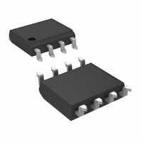
LM5002MA/NOPB National Semiconductor, LM5002MA/NOPB Datasheet

LM5002MA/NOPB
Specifications of LM5002MA/NOPB
Available stocks
Related parts for LM5002MA/NOPB
LM5002MA/NOPB Summary of contents
Page 1
... Addi- tional protection features include: current limit, thermal shutdown, under-voltage lockout and remote shutdown ca- pability. The device is available in both SO-8 and LLP-8 packages. Typical Application Circuit © 2009 National Semiconductor Corporation LM5002 Features ■ Integrated 75 volt N-Channel MOSFET ■ ...
Page 2
Connection Diagrams Top View SO-8 Package Ordering Information Order Number LM5002MA LM5002MAX LM5002SD LM5002SDX Pin Descriptions Pin Name Description SO LLP Switch pin 2 4 VIN Input supply pin 3 5 VCC Bias regulator output, or input ...
Page 3
Pin Name Description SO LLP Enable / Under Voltage Lock-Out / Shutdown input Exposed Pad, LLP only Application Information An external voltage divider can be used to set the line undervoltage lockout threshold. If ...
Page 4
... Absolute Maximum Ratings If Military/Aerospace specified devices are required, please contact the National Semiconductor Sales Office/ Distributors for availability and specifications. VIN to GND SW to GND (Steady State) VCC GND COMP, FB GND Maximum Junction Temperature Electrical Characteristics junction temperature (T ) range of -40°C to +125°C. Minimum and Maximum limits are guaranteed through test, design, or statistical J correlation ...
Page 5
Symbol Parameter ERROR AMPLIFIER V Feedback Reference Voltage FB-REF FB Bias Current DC Gain COMP Sink Current COMP Short Circuit Current COMP Open Circuit Voltage COMP to SW Delay Unity Gain Bandwidth THERMAL SHUTDOWN T Thermal Shutdown Threshold SD Thermal ...
Page 6
Typical Performance Characteristics Efficiency, Boost Converter I (non-switching DS(ON) www.national.com 30004518 IN 30004520 CC 30004522 Temperature FB 30004519 30004521 R vs Temperature DS(ON) 30004523 ...
Page 7
LIM CC 30004524 30004526 30004528 Temperature LIM CC 30004525 F vs Temperature SW 30004527 Temperature EN VIN 30004529 ...
Page 8
Block Diagram Functional Description The LM5002 high voltage switching regulator features all the functions necessary to implement an efficient boost, flyback, SEPIC or forward current mode power converter. The oper- ation can be best understood by referring to the block ...
Page 9
The controller remains enabled until VCC falls below 2.7V or the EN pin falls below 1.16V. An auxiliary supply voltage can be applied to the VCC pin to reduce the IC power dissipation. If the auxiliary voltage is ...
Page 10
When isolation between primary and secondary circuits is re- quired, the Error Amplifier is usually disabled by connecting the FB pin to GND. This allows the COMP pin to be driven directly by the collector of an opto-coupler. In isolated ...
Page 11
Application Information The following information is intended to provide guidelines for the power supply designer using the LM5002. VIN The voltage applied to the VIN pin can vary within the range of 3.1V to 75V. The current into the VIN ...
Page 12
Remote configuration of the controller’s operational modes can be accomplished with open drain device(s) connected to the EN pin as shown in Figure 4. A MOSFET or an NPN tran- sistor connected to the EN pin can force the regulator ...
Page 13
FIGURE 5. Soft-Start 13 30004512 www.national.com ...
Page 14
Printed Circuit Board Layout The LM5002 Current Sense and PWM comparators are very fast and may respond to short duration noise pulses. The components at the SW, COMP, EN and the RT pins should be as physically close as possible ...
Page 15
FIGURE 6. Non-Isolated Flyback FIGURE 7. Isolated Flyback 15 30004513 30004514 www.national.com ...
Page 16
FIGURE 8. Boost FIGURE 9. 24V SEPIC FIGURE 10. 12V SEPIC 16 30004515 30004516 30004517 ...
Page 17
Physical Dimensions inches (millimeters) unless otherwise noted 8-Lead SO-8 Package NS Package Number M08A 8-Lead LLP Package NS Package Number SDC08A 17 www.national.com ...
Page 18
... For more National Semiconductor product information and proven design tools, visit the following Web sites at: Products Amplifiers www.national.com/amplifiers Audio www.national.com/audio Clock and Timing www.national.com/timing Data Converters www.national.com/adc Interface www.national.com/interface LVDS www.national.com/lvds Power Management www.national.com/power Switching Regulators www.national.com/switchers LDOs www.national.com/ldo LED Lighting www ...


