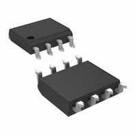
LM5002MA/NOPB National Semiconductor, LM5002MA/NOPB Datasheet - Page 2

LM5002MA/NOPB
Manufacturer Part Number
LM5002MA/NOPB
Description
IC REG SWITCH MODE HV 8-SOIC
Manufacturer
National Semiconductor
Type
Step-Up (Boost), Flyback, Forward Converter, Sepicr
Datasheet
1.LM5002SDNOPB.pdf
(18 pages)
Specifications of LM5002MA/NOPB
Internal Switch(s)
Yes
Synchronous Rectifier
No
Number Of Outputs
1
Current - Output
500mA
Frequency - Switching
1.5MHz
Voltage - Input
3.1 ~ 75 V
Operating Temperature
-40°C ~ 125°C
Mounting Type
Surface Mount
Package / Case
8-SOIC (3.9mm Width)
Lead Free Status / RoHS Status
Lead free / RoHS Compliant
Voltage - Output
-
Power - Output
-
Other names
LM5002MA
Available stocks
Company
Part Number
Manufacturer
Quantity
Price
Part Number:
LM5002MA/NOPB
Manufacturer:
NS/国半
Quantity:
20 000
www.national.com
Connection Diagrams
Ordering Information
Pin Descriptions
SO
1
2
3
4
5
6
7
Pin
LLP
Order Number
LM5002MAX
LM5002SDX
3
4
5
6
7
8
1
LM5002MA
LM5002SD
COMP
Name
GND
VCC
SW
VIN
RT
FB
SO-8 Package
Top View
Description
Switch pin
Input supply pin
Bias regulator output, or input for external
bias supply
Ground
Oscillator frequency programming and
optional synchronization pulse input
Feedback input from the regulated output
voltage
Open drain output of the internal error
amplifier
Package Type
LLP-8
LLP-8
SO-8
SO-8
30004502
2
NSC Package Drawing
Application Information
The drain terminal of the internal power MOSFET.
Nominal operating range: 3.1V to 75V.
VCC tracks VIN up to 6.9V. Above VIN = 6.9V, VCC is
regulated to 6.9 Volts. A 0.47 µF or greater ceramic
decoupling capacitor is required. An external voltage (7V –
12V) can be applied to this pin which disables the internal
VCC regulator to reduce internal power dissipation and
improve converter efficiency.
Internal reference for the regulator control functions and the
power MOSFET current sense resistor connection.
The internal oscillator is set with a resistor, between this pin
and the GND pin. The recommended frequency range is
50KHz to 1.5 MHz. The RT pin can accept synchronization
pulses from an external clock. A 100 pF capacitor is
recommended for coupling the synchronizing clock to the
RT pin.
This pin is connected to the inverting input of the internal
error amplifier. The 1.26V reference is internally connected
to the non-inverting input of the error amplifier.
The loop compensation network should be connected
between the COMP pin and the FB pin. COMP pull-up is
provided by an internal 5 kΩ resistor which may be used to
bias an opto-coupler transistor (while FB is grounded) for
isolated ground applications.
SDC08A
SDC08A
M08A
M08A
LLP-8 Package
Top View
2500 Units on Tape and Reel
1000 Units on Tape and Reel
4500 Units on Tape and Reel
95 Units in a Rail
Supplied As
30004503


