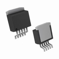
LM2596S-ADJ/NOPB National Semiconductor, LM2596S-ADJ/NOPB Datasheet - Page 25

LM2596S-ADJ/NOPB
Manufacturer Part Number
LM2596S-ADJ/NOPB
Description
IC REG SIMPLE SWITCHER TO-263-5
Manufacturer
National Semiconductor
Series
SIMPLE SWITCHER®r
Type
Step-Down (Buck)r
Datasheets
1.LM2596S-ADJNOPB.pdf
(31 pages)
2.LM2587S-ADJNOPB.pdf
(28 pages)
3.LM2596S-ADJNOPB.pdf
(6 pages)
Specifications of LM2596S-ADJ/NOPB
Internal Switch(s)
Yes
Synchronous Rectifier
No
Number Of Outputs
1
Voltage - Output
1.2 ~ 37 V
Current - Output
3A
Frequency - Switching
150kHz
Voltage - Input
4.5 ~ 40 V
Operating Temperature
-40°C ~ 125°C
Mounting Type
Surface Mount
Package / Case
D²Pak, TO-263 (5 leads + tab)
Current, Input Bias
10 nA
Current, Output
3 A
Current, Supply
5 mA
Frequency, Oscillator
150 kHz
Package Type
TO-263
Regulator Type
Buck, Switching
Resistance, Thermal, Junction To Case
2 °C/W
Temperature, Operating, Range
-40 to +125 °C
Voltage, Input
4.5 to 40 V
Voltage, Output
1.2 to 37 V
Primary Input Voltage
40V
No. Of Outputs
1
Output Voltage
37V
Output Current
3A
No. Of Pins
5
Operating Temperature Range
-40°C To +125°C
Msl
MSL 3 - 168 Hours
Filter Terminals
SMD
Rohs Compliant
Yes
For Use With
551011367-041 - BOARD WEBENCH BUILD IT
Lead Free Status / RoHS Status
Lead free / RoHS Compliant
Power - Output
-
Lead Free Status / Rohs Status
RoHS Compliant part
Other names
*LM2596S-ADJ
*LM2596S-ADJ/NOPB
LM2596S-ADJ
*LM2596S-ADJ/NOPB
LM2596S-ADJ
Available stocks
Company
Part Number
Manufacturer
Quantity
Price
Company:
Part Number:
LM2596S-ADJ/NOPB
Manufacturer:
TI
Quantity:
25
4) LM2587 package thermal resistances θ
in the Electrical Characteristics).
Total power dissipated (P
as follows:
Boost:
V
N is the transformer turns ratio, D is the duty cycle, and
I
the maximum load currents for multiple-output flyback regu-
lators). The duty cycle is given by:
Boost:
where V
typically 0.5V for Schottky diodes and 0.8V for fast recovery
diodes. V
in the Characteristic Curves.
When no heat sink is used, the junction temperature rise is:
Adding the junction temperature rise to the maximum ambient
temperature gives the actual operating junction temperature:
If the operating junction temperature exceeds the maximum
junction temperatue in item 3 above, then a heat sink is re-
LOAD
IN
is the minimum input voltage, V
is the maximum load current (and
F
SAT
is the forward biased voltage of the diode and is
is the switch saturation voltage and can be found
ΔT
T
J
D
J
= ΔT
) by the LM2587 can be estimated
= P
D
J
× θ
+ T
OUT
JA
A
.
.
is the output voltage,
∑
I
LOAD
JA
and θ
is the sum of
JC
(given
25
quired. When using a heat sink, the junction temperature rise
can be determined by the following:
Again, the operating junction temperature will be:
As before, if the maximum junction temperature is exceeded,
a larger heat sink is required (one that has a lower thermal
resistance).
Included in the Switchers Made Simple design software is a
more precise (non-linear) thermal model that can be used to
determine junction temperature with different input-output pa-
rameters or different component values. It can also calculate
the heat sink thermal resistance required to maintain the reg-
ulator junction temperature below the maximum operating
temperature.
To further simplify the flyback regulator design procedure,
National Semiconductor is making available computer design
software. Switchers Made Simple software is available on
a (3½ ) diskette for IBM compatable computers from a Na-
tional Semiconductor sales office in your area or the National
Semiconductor
(1-800-272-9959).
European Magnetic Vendor
Contacts
Please contact the following addresses for details of local
distributors or representatives:
Coilcraft
21 Napier Place
Wardpark North Cumbernauld, Scotland G68 0LL Phone: +44
1236 730 595 Fax: +44 1236 730 627
Pulse Engineering
Dunmore Road
Tuam Co. Galway, Ireland Phone: +353 93 24 107 Fax: +353
93 24 459
ΔT
J
= P
D
× (θ
Customer
T
J
JC
= ΔT
+ θ
Interface
J
+ T
A
Response
+ θ
Heat Sink
)
www.national.com
Center


