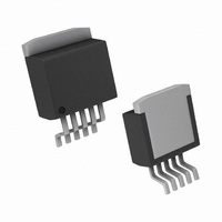
LM2596S-ADJ/NOPB National Semiconductor, LM2596S-ADJ/NOPB Datasheet - Page 3

LM2596S-ADJ/NOPB
Manufacturer Part Number
LM2596S-ADJ/NOPB
Description
IC REG SIMPLE SWITCHER TO-263-5
Manufacturer
National Semiconductor
Series
SIMPLE SWITCHER®r
Type
Step-Down (Buck)r
Datasheets
1.LM2596S-ADJNOPB.pdf
(31 pages)
2.LM2587S-ADJNOPB.pdf
(28 pages)
3.LM2596S-ADJNOPB.pdf
(6 pages)
Specifications of LM2596S-ADJ/NOPB
Internal Switch(s)
Yes
Synchronous Rectifier
No
Number Of Outputs
1
Voltage - Output
1.2 ~ 37 V
Current - Output
3A
Frequency - Switching
150kHz
Voltage - Input
4.5 ~ 40 V
Operating Temperature
-40°C ~ 125°C
Mounting Type
Surface Mount
Package / Case
D²Pak, TO-263 (5 leads + tab)
Current, Input Bias
10 nA
Current, Output
3 A
Current, Supply
5 mA
Frequency, Oscillator
150 kHz
Package Type
TO-263
Regulator Type
Buck, Switching
Resistance, Thermal, Junction To Case
2 °C/W
Temperature, Operating, Range
-40 to +125 °C
Voltage, Input
4.5 to 40 V
Voltage, Output
1.2 to 37 V
Primary Input Voltage
40V
No. Of Outputs
1
Output Voltage
37V
Output Current
3A
No. Of Pins
5
Operating Temperature Range
-40°C To +125°C
Msl
MSL 3 - 168 Hours
Filter Terminals
SMD
Rohs Compliant
Yes
For Use With
551011367-041 - BOARD WEBENCH BUILD IT
Lead Free Status / RoHS Status
Lead free / RoHS Compliant
Power - Output
-
Lead Free Status / Rohs Status
RoHS Compliant part
Other names
*LM2596S-ADJ
*LM2596S-ADJ/NOPB
LM2596S-ADJ
*LM2596S-ADJ/NOPB
LM2596S-ADJ
Available stocks
Company
Part Number
Manufacturer
Quantity
Price
Company:
Part Number:
LM2596S-ADJ/NOPB
Manufacturer:
TI
Quantity:
25
SYSTEM PARAMETERS Test Circuit of
V
ΔV
ΔV
ΔV
ΔI
η
UNIQUE DEVICE PARAMETERS
V
ΔV
G
A
SYSTEM PARAMETERS Test Circuit of
V
ΔV
ΔV
ΔV
ΔI
η
UNIQUE DEVICE PARAMETERS
V
ΔV
G
A
OUT
REF
VOL
Symbol
OUT
REF
VOL
M
M
Symbol
LOAD
LOAD
LM2587-5.0
Electrical Characteristics
Specifications with standard type face are for T
Range. Unless otherwise specified, V
LM2587-12
Electrical Characteristics
Specifications with standard type face are for T
Range. Unless otherwise specified, V
OUT
IN
OUT
REF
OUT
IN
OUT
REF
/
/
/
/
Output Voltage
Line Regulation
Load Regulation
Efficiency
Output Reference
Voltage
Reference Voltage
Line Regulation
Error Amp
Transconductance
Error Amp
Voltage Gain
Output Voltage
Line Regulation
Load Regulation
Efficiency
Output Reference
Voltage
Reference Voltage
Line Regulation
Error Amp
Transconductance
Error Amp
Voltage Gain
Parameters
Parameters
(Note
(Note
V
I
V
I
V
I
V
Measured at Feedback Pin
V
V
I
V
V
R
LOAD
LOAD
LOAD
COMP
V
I
V
I
V
I
V
Measured at Feedback Pin
V
V
I
V
V
R
LOAD
LOAD
LOAD
COMP
IN
IN
IN
IN
COMP
IN
COMP
COMP
COMP
IN
IN
IN
IN
COMP
IN
COMP
COMP
COMP
IN
IN
Figure 2 (Note
Figure 3 (Note
5)
5)
= 4V to 12V
= 4V to 12V
= 12V
= 12V, I
= 4V to 40V
= 4V to 10V
= 4V to 10V
= 10V
= 10V, I
= 4V to 40V
= 5V.
= 5V.
= 500 mA to 1.45A
= 500 mA
= 500 mA to 1.45A
= −30 μA to +30 μA
= 300 mA to 1.2A
= 300 mA
= 300 mA to 1.2A
= −30 μA to +30 μA
= 1.0V
= 1.0V
= 0.5V to 1.6V
= 1.0 MΩ
= 1.0V
= 1.0V
= 0.5V to 1.6V
= 1.0 MΩ
Conditions
Conditions
LOAD
LOAD
J
J
= 25°C, and those in bold type face apply over full Operating Temperature
= 25°C, and those in bold type face apply over full Operating Temperature
= 750 mA
(Note
= 1A
(Note
4)
4)
6)
6)
3
Typical
0.328
Typical
12.0
12.0
7.8
0.750
20
20
90
70
165
5.0
5.0
3.3
20
20
80
11.52/11.40
11.79/11.76
4.913/4.900
4.80/4.75
0.186
41/21
Min
0.447
99/49
Min
5.088/5.100
12.48/12.60
12.21/12.24
5.20/5.25
100/200
100/200
50/100
50/100
1.491
0.621
Max
Max
www.national.com
mmho
Units
mmho
Units
mV
mV
mV
V/V
mV
mV
mV
V/V
%
V
V
%
V
V


