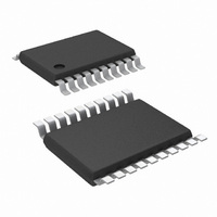
LM5116MH/NOPB National Semiconductor, LM5116MH/NOPB Datasheet - Page 18

LM5116MH/NOPB
Manufacturer Part Number
LM5116MH/NOPB
Description
IC CTRLR SYNCH BUCK 20-TSSOP
Manufacturer
National Semiconductor
Series
PowerWise®r
Type
Step-Down (Buck)r
Datasheet
1.LM5116MHNOPB.pdf
(26 pages)
Specifications of LM5116MH/NOPB
Internal Switch(s)
No
Synchronous Rectifier
Yes
Number Of Outputs
1
Voltage - Output
1.22 ~ 80 V
Current - Output
20A
Frequency - Switching
50kHz ~ 1MHz
Voltage - Input
6 ~ 100 V
Operating Temperature
-40°C ~ 125°C
Mounting Type
Surface Mount
Package / Case
20-TSSOP Exposed Pad, 20-eTSSOP, 20-HTSSOP
Dc To Dc Converter Type
Synchronous Buck Controller
Pin Count
20
Input Voltage
6 to 100V
Output Voltage
1.215 to 80V
Output Current
3.5A
Package Type
TSSOP EP
Mounting
Surface Mount
Operating Temperature Classification
Automotive
Operating Temperature (min)
-40C
Operating Temperature (max)
125C
For Use With
LM5116-12EVAL - BOARD EVALUATION FOR LM5116-12LM5116EVAL - BOARD EVALUATION LM5116
Lead Free Status / RoHS Status
Lead free / RoHS Compliant
Power - Output
-
Lead Free Status / Rohs Status
Compliant
Other names
LM5116MH
www.national.com
The converter exhibits a negative input impedance which is
lowest at the minimum input voltage:
The damping factor for the input filter is given by:
Where R
resistance of the input capacitors. The term Z
be negative due to Z
When δ = 1, the input filter is critically damped. This may be
difficult to achieve with practical component values. With δ <
0.2, the input filter will exhibit significant ringing. If δ is zero or
negative, there is not enough resistance in the circuit and the
input filter will sustain an oscillation. When operating near the
minimum input voltage, an aluminum electrolytic capacitor
across C
bench test setup. Any parallel capacitor should be evaluated
for its RMS current rating. The current will split between the
ceramic and aluminum capacitors based on the relative
impedance at the switching frequency.
VCC CAPACITOR
The primary purpose of the VCC capacitor (C
the peak transient currents of the LO driver and bootstrap
diode (D1) as well as provide stability for the VCC regulator.
These current peaks can be several amperes. The recom-
mended value of C
should be a good quality, low ESR, ceramic capacitor located
at the pins of the IC to minimize potentially damaging voltage
transients caused by trace inductance. A value of 1µF was
selected for this design.
BOOTSTRAP CAPACITOR
The bootstrap capacitor (C
supplies the gate current to charge the high-side MOSFET
gate at each cycle’s turn-on as well as supplying the recovery
charge for the bootstrap diode (D1). These current peaks can
be several amperes. The recommended value of the boot-
strap capacitor is at least 0.1µF, and should be a good quality,
low ESR, ceramic capacitor located at the pins of the IC to
minimize potentially damaging voltage transients caused by
trace inductance. The absolute minimum value for the boot-
strap capacitor is calculated as:
Where Q
the tolerable voltage droop on C
5% of VCC. A value of 1µF was selected for this design.
IN
g
IN
is the high-side MOSFET gate charge and ΔV
is the input wiring resistance and ESR is the series
may be needed to damp the input for a typical
VCC
IN
.
should be no smaller than 0.47µF, and
HB
) between the HB and SW pins
HB
, which is typically less than
S
VCC
/ Z
IN
) is to supply
will always
HB
is
18
SOFT START CAPACITOR
The capacitor at the SS pin (C
time, which is the time for the reference voltage and the output
voltage to reach the final regulated value. The soft-start time
t
charge C
this requirement:
The value of C
For this application, a value of 0.01µF was chosen for a soft-
start time of 1.2ms.
OUTPUT VOLTAGE DIVIDER
R
resistors is calculated from:
R
vider current can be reduced to 100µA with R
the 5V output design example used here, R
R
UVLO DIVIDER
A voltage divider and filter can be connected to the UVLO pin
to set a minimum operating voltage V
If this feature is required, the following procedure can be used
to determine appropriate resistor values for R
C
1.
2.
3.
If under-voltage shutdown is not required, R
be eliminated and the off-time becomes:
SS
FB1
FB1
FB2
FT
should be substantially longer than the time required to
.
R
current limit, the internal UVLO switch can pull UVLO <
200mV. This can be guaranteed if:
Where V
is in ohms.
2. With an appropriate value for R
selected using the following equation:
Where V
Capacitor C
determines the off-time of the “hiccup” duty cycle during
current limit. When C
voltage divider, a diode across the top resistor should be
used to discharge C
voltage condition.
and R
= 3.74kΩ.
is typically 1.21kΩ for a divider current of 1mA. The di-
UV2
OUT
t
must be large enough such that in the event of a
SS
FB2
to V
> V
IN(MAX)
IN(MIN)
SS
set the output voltage level, the ratio of these
FT
OUT
OUT
for a given time is determined from:
provides filtering for the divider and
is the desired shutdown voltage.
is the maximum input voltage and R
x C
at the maximum output current. To meet
R
UV2
OUT
FT
FT
> 500 x V
in the event of an input under-
/ (I
is used in conjunction with the
CURRENT LIMIT
SS
) determines the soft-start
IN(MAX)
IN(MIN)
UV2
, R
FB1
UV1
for the regulator.
– I
FB1
UV1
OUT
UV2
= 1.21kΩ and
and R
=12.1kΩ. For
can be
, R
)
UV1
UV2
UV2
and
can


