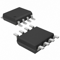
MAX682ESA+ Maxim Integrated Products, MAX682ESA+ Datasheet - Page 5

MAX682ESA+
Manufacturer Part Number
MAX682ESA+
Description
IC CHARGE PUMP 5V 8-SOIC
Manufacturer
Maxim Integrated Products
Type
Switched Capacitor (Charge Pump)r
Datasheet
1.MAX682ESA.pdf
(12 pages)
Specifications of MAX682ESA+
Internal Switch(s)
Yes
Synchronous Rectifier
No
Number Of Outputs
1
Voltage - Output
5V
Current - Output
250mA
Frequency - Switching
200kHz, 1MHz
Voltage - Input
2.7 ~ 5.5 V
Operating Temperature
-40°C ~ 85°C
Mounting Type
Surface Mount
Package / Case
8-SOIC (3.9mm Width)
Power - Output
471mW
Function
Step Up
Output Voltage
5.05 V
Output Current
250 mA (Min)
Supply Current
0.18 mA
Maximum Operating Temperature
+ 85 C
Minimum Operating Temperature
- 40 C
Mounting Style
SMD/SMT
Lead Free Status / RoHS Status
Lead free / RoHS Compliant
(Circuit of Figure 5, V
A: OUTPUT VOLTAGE: SKIP = HIGH, R
B: SHDN VOLTAGE: 1V/div
PIN
1
2
3
4
5
6
7
8
NAME
SHDN
PGND
GND
CXN
OUT
SKIP
CXP
SHUTDOWN TIMING
IN
100 s/div
_______________________________________________________________________________________
IN
When SKIP = low, the regulator operates in low-quiescent-current skip mode. When SKIP = high, the
regulator operates in constant-frequency mode, minimizing output ripple and noise. SKIP must be tied
high for input voltages above 3.6V.
Shutdown Input. Drive SHDN through an external resistor. When SHDN = low, the device turns off. When
current is sourced into SHDN through R
oscillator’s switching frequency. R
Input Supply Pin. Can range from 2.7V to 5.5V for SKIP = high, and 2.7V to 3.6V for SKIP = low. Bypass to
PGND with a suitable value capacitor (see Capacitor Selection section).
Ground Pin. Connect to PGND through a short trace.
Power Ground Pin
Negative Terminal of the Charge-Pump Transfer Capacitor
Positive Terminal of the Charge-Pump Transfer Capacitor
Fixed 5V Power Output. Bypass to PGND with output filter capacitor.
= 3.3V, component values from Tables 2 and 3, T
L
= 5V / I
MAX682 TOC18
MAX
, 2V/div
3.3V-Input to Regulated 5V-Output
A
B
Typical Operating Characteristics (continued)
A: INPUT VOLTAGE: V
B: OUTPUT VOLTAGE: SKIP = HIGH, I
I
LOAD
= 250mA, 50mV/div, MAX682
LINE-TRANSIENT RESPONSE
EXT
(kΩ) = 45000 (V
EXT
IN
2ms/div
= 3.1V TO 3.6V, 500mV/div
, the device activates, and the SHDN pin input current sets the
FUNCTION
A
SHDN
= +25°C, unless otherwise noted.)
= 22 A,
IN
MAX682 TOC20
- 0.69V) / f
A
B
OSC
Charge Pumps
A: LOAD CURRENT: I
B: OUTPUT VOLTAGE: SKIP = HIGH, I
(kHz).
100mV/div, MAX682
LOAD-TRANSIENT RESPONSE
Pin Description
LOAD
2ms/div
= 5mA TO 250mA, 500mA/div
SHDN
= 22 A,
MAX682 TOC19
5
A
B


