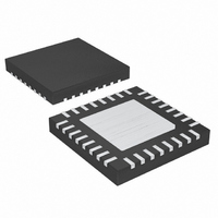
MAX8833ETJ+ Maxim Integrated Products, MAX8833ETJ+ Datasheet - Page 13

MAX8833ETJ+
Manufacturer Part Number
MAX8833ETJ+
Description
IC REG STP DWN DUAL 3A 32-TQFN
Manufacturer
Maxim Integrated Products
Type
Step-Down (Buck)r
Datasheet
1.MAX8833ETJ.pdf
(20 pages)
Specifications of MAX8833ETJ+
Internal Switch(s)
Yes
Synchronous Rectifier
No
Number Of Outputs
2
Voltage - Output
0.6 ~ 3.24 V
Current - Output
3A
Frequency - Switching
500kHz ~ 2MHz
Voltage - Input
2.35 ~ 3.6 V
Operating Temperature
-40°C ~ 85°C
Mounting Type
Surface Mount
Package / Case
32-TQFN Exposed Pad
Power - Output
2.76W
Output Voltage
0.6 V to 0.9 V
Output Current
3 A
Input Voltage
2.35 V to 3.6 V
Switching Frequency
2 MHz
Operating Temperature Range
- 40 C to + 85 C
Mounting Style
SMD/SMT
Duty Cycle (max)
95 %
Lead Free Status / RoHS Status
Lead free / RoHS Compliant
In DDR tracking applications such as Figure 7, the FB1
regulation voltage tracks the voltage at REFIN. In Figure
7, the output of regulator 1 tracks V
of the output voltages is set as follows:
The MAX8833 has an adjustable internal oscillator that
can be set to any frequency from 500kHz to 2MHz. To
set the switching frequency, connect a resistor from
FSYNC to GND. Calculate the resistor value from the
following equation:
The MAX8833 can also be synchronized to an external
clock from 500kHz to 2MHz by connecting the clock
signal to FSYNC through a 10kΩ isolation resistor. The
external sync frequency must be higher than the fre-
quency that would be produced by R
regulators switch at the same frequency as the FSYNC
clock, and are 180° out-of-phase with each other. The
external clock duty cycle may range between 10% and
90% to ensure 180° out-of-phase operation.
The two step-down regulators have independent
adjustable soft-start. Capacitors from SS_ to GND are
charged from a constant 8μA (typ) current source to the
feedback-regulation voltage. The value of the soft-start
capacitors is calculated from the desired soft-start time
as follows:
There are several parameters that must be examined
when determining which inductor to use: maximum
input voltage, output voltage, load current, switching
frequency, and LIR. LIR is the ratio of inductor current
ripple to DC load current. A higher LIR value allows for
a smaller inductor, but results in higher losses and
higher output ripple. On the other hand, higher inductor
values increase efficiency, but eventually resistive loss-
es due to extra turns of wire exceed the benefit gained
from lower AC current levels. A good compromise
between size and efficiency is a 30% LIR. For applica-
tions in which size and transient response are impor-
R
Setting the Switching Frequency
FSYNC
C
______________________________________________________________________________________
V
V
SS
OUT
OUT
Setting the Soft-Start Time
=
_
⎛
⎜
⎝
=
2
1
f
1
S
t
=
SS
Dual, 3A, 2MHz Step-Down Regulator
−
R
50
1
×
R
ns
+
⎛
⎜
⎝
Inductor Selection
19
0 6
8
⎞
⎟
⎠
R
.
μ
⎛
⎜
⎝
19
A
V
950
10
OUT2
⎞
⎟
⎠
k
ns
Ω
FSYNC
, and the ratio
⎞
⎟
⎠
. The two
tant, an LIR of around 40% to 50% is recommended.
Once all the parameters are chosen, the inductor value
is determined as follows:
where f
value close to the calculated value. The exact inductor
value is not critical and can be adjusted to make trade-
offs among size, cost, and efficiency. Find a low-loss
inductor with the lowest possible DC resistance that fits
the allotted dimensions. The peak inductor current is
determined as:
I
current rating or the minimum current-limit specification
for the MAX8833.
The input capacitor for each regulator serves to reduce
the current peaks drawn from the input power supply
and reduces switching noise in the IC. The total input
capacitance for each rail must be equal to or greater
than the value given by the following equation to keep
the input-voltage ripple within specifications and mini-
mize the high-frequency ripple current being fed back
to the input source:
where D_ is the quiescent duty cycle (V
is the switching frequency; and V
to-peak input-voltage ripple, which should be less than
2% of the minimum DC input voltage.
The impedance of the input capacitor at the switching
frequency should be less than that of the input source
so high-frequency switching currents do not pass
through the input source but are instead shunted
through the input capacitor. High source impedance
requires high-input capacitance. The input capacitor
must meet the ripple current requirement imposed by
the switching currents. The RMS input ripple current,
I
PEAK
RIPPLE_
must not exceed the chosen inductor’s saturation
S
, is given by:
is the switching frequency. Choose a standard
I
RIPPLE
C
L
I
IN MIN
PEAK
=
_
f
S
_
×
V
=
=
OUT
V
_
I
⎛
⎜
⎝
OUT
IN
1
Input-Capacitor Selection
=
+
×
f
×
SW
LIR
LIR I
_
2
(
V
×
D
IN
⎞
⎟ ×
⎠
×
×
_
D
−
V
OUT MAX
I
×
IN RIPPLE
OUT MAX
V
_
IN_RIPPLE
OUT
I
_
×
OUT
(
(
(
1
)
−
_
OUT_
D
)
)
_)
_
is the peak-
/V
IN_
); f
SW
13


