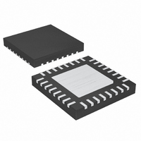
MAX8833ETJ+ Maxim Integrated Products, MAX8833ETJ+ Datasheet - Page 14

MAX8833ETJ+
Manufacturer Part Number
MAX8833ETJ+
Description
IC REG STP DWN DUAL 3A 32-TQFN
Manufacturer
Maxim Integrated Products
Type
Step-Down (Buck)r
Datasheet
1.MAX8833ETJ.pdf
(20 pages)
Specifications of MAX8833ETJ+
Internal Switch(s)
Yes
Synchronous Rectifier
No
Number Of Outputs
2
Voltage - Output
0.6 ~ 3.24 V
Current - Output
3A
Frequency - Switching
500kHz ~ 2MHz
Voltage - Input
2.35 ~ 3.6 V
Operating Temperature
-40°C ~ 85°C
Mounting Type
Surface Mount
Package / Case
32-TQFN Exposed Pad
Power - Output
2.76W
Output Voltage
0.6 V to 0.9 V
Output Current
3 A
Input Voltage
2.35 V to 3.6 V
Switching Frequency
2 MHz
Operating Temperature Range
- 40 C to + 85 C
Mounting Style
SMD/SMT
Duty Cycle (max)
95 %
Lead Free Status / RoHS Status
Lead free / RoHS Compliant
Dual, 3A, 2MHz Step-Down Regulator
The key selection parameters for the output capacitor
are capacitance, ESR, ESL, and voltage-rating require-
ments. These affect the overall stability, output ripple
voltage, and transient response of the DC-DC convert-
er. The output ripple occurs due to variations in the
charge stored in the output capacitor, the voltage drop
due to the capacitor’s ESR, and the voltage drop due to
the capacitor’s ESL. Calculate the output-voltage ripple
due to the output capacitance, ESR, and ESL as:
where the output ripple due to output capacitance,
ESR, and ESL is:
or:
whichever is greater.
It should be noted that the above ripple voltage compo-
nents add vectrorially rather than algebraically, thus
making V
The peak inductor current (I
Use these equations for initial capacitor selection.
Determine final values by testing a prototype or an eval-
uation circuit. A smaller ripple current results in less out-
put-voltage ripple. Since the inductor ripple current is a
function of the inductor value, the output-voltage ripple
decreases with larger inductance. Use ceramic capaci-
tors for low ESR and low ESL at the switching frequency
of the converter. The low ESL of ceramic capacitors
makes ripple voltages due to ESL negligible.
Load-transient response depends on the selected out-
put capacitance. During a load transient, the output
instantly changes by ESR x ΔI
troller can respond, the output deviates further,
depending on the inductor and output capacitor values.
14
V
RIPPLE
______________________________________________________________________________________
RIPPLE
=
V
RIPPLE C
I
V
V
P P
V
V
RIPPLE C
RIPPLE ESL
a conservative estimate.
−
RIPPLE ESR
RIPPLE ESL
=
Output-Capacitor Selection
( )
V
IN
( )
(
(
(
+
f
S
−
V
=
×
)
V
RIPPLE ESR
)
)
OUT
8
=
P-P
L
=
=
×
t
I
I
I
P P
P P
OFF
t
C
P P
) is:
ON
−
−
I
−
LOAD
P P
OUT
×
(
−
V
×
×
×
OUT
V
ESR
ESL
ESL
IN
×
)
. Before the con-
+
f
S
V
RIPPLE ESL
(
)
After a short time, the controller responds by regulating
the output voltage back to its predetermined value. The
controller response time depends on the closed-loop
bandwidth. A higher bandwidth yields a faster
response time, preventing the output from deviating fur-
ther from its regulating value. See the Compensation
Design and Safe-Starting into a Prebiased Output sec-
tions for more details.
The power-stage transfer function consists of one dou-
ble pole and one zero. The double pole is introduced
by the output filtering inductor, L, and the output filter-
ing capacitor, C
capacitor determines the zero. The double pole and
zero frequencies are given as follows:
where R
DC resistance and the internal switch resistance,
R
output load resistance, which is equal to the rated out-
put voltage divided by the rated output current. ESR is
the total ESR of the output-filtering capacitor. If there is
more than one output capacitor of the same type in par-
allel, the value of the ESR in the above equation is
equal to that of the ESR of a single-output capacitor
divided by the total number of output capacitors.
The high-switching-frequency range of the MAX8833
allows the use of ceramic output capacitors. Since the
ESR of ceramic capacitors is typically very low, the fre-
quency of the associated transfer-function zero is high-
er than the unity-gain crossover frequency, f
zero cannot be used to compensate for the double pole
created by the output filtering inductor and capacitor.
The double pole produces a gain drop of 40dB and a
phase shift of 180° per decade. The error amplifier
must compensate for this gain drop and phase shift to
achieve a stable high-bandwidth closed-loop system.
Therefore, use type III compensation as shown in
Figure 4. Type III compensation possesses three poles
and two zeros with the first pole, f
(DC). Locations of other poles and zeros of type III
compensation are given by:
DS(ON)
f
P LC
1
. A typical value for R
_
L
is equal to the sum of the output inductor’s
=
f
P
2
f
Z ESR
_
f
Z EA
_
LC
O
1
. The ESR of the output filtering
_
=
2
=
=
π
2π
×
2
π
Compensation Design
×
L C
×
DS(ON)
ESR C
R
×
1
1
7
×
O
P1_EA
×
C
1
×
9
is 35mΩ. R
O
⎛
⎜
⎝
R
R
, located at 0Hz
O
O
+
+
ESR
R
C
L
, and the
⎞
⎟
⎠
O
is the


