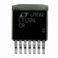
LT1374CR#PBF Linear Technology, LT1374CR#PBF Datasheet - Page 8

LT1374CR#PBF
Manufacturer Part Number
LT1374CR#PBF
Description
IC SW REG 4.5A ADJ STEP-DWN 7-DD
Manufacturer
Linear Technology
Type
Step-Down (Buck)r
Datasheet
1.LT1374CFEPBF.pdf
(32 pages)
Specifications of LT1374CR#PBF
Internal Switch(s)
Yes
Synchronous Rectifier
No
Number Of Outputs
1
Voltage - Output
2.42 ~ 21.5 V
Current - Output
4.5A
Frequency - Switching
500kHz
Voltage - Input
5 ~ 25 V
Operating Temperature
0°C ~ 125°C
Mounting Type
Surface Mount
Package / Case
D²Pak, TO-263 (7 leads + tab)
Primary Input Voltage
25V
No. Of Outputs
1
Output Current
4.5A
No. Of Pins
7
Operating Temperature Range
0°C To +125°C
Msl
MSL 1 - Unlimited
Supply Voltage Range
5V To 25V
Rohs Compliant
Yes
Lead Free Status / RoHS Status
Lead free / RoHS Compliant
Power - Output
-
Available stocks
Company
Part Number
Manufacturer
Quantity
Price
BLOCK DIAGRA
LT1374
APPLICATIO S I FOR ATIO
FEEDBACK PIN FUNCTIONS
The feedback (FB) pin on the LT1374 is used to set output
voltage and provide several overload protection features.
The first part of this section deals with selecting resistors
to set output voltage and the remaining part talks about
foldback frequency and current limiting created by the FB
pin. Please read both parts before committing to a final
design. The fixed 5V LT1374-5 has internal divider resis-
tors and the FB pin is renamed SENSE, connected directly
to the output.
The suggested value for the output divider resistor (see
Figure 2) from FB to ground (R2) is 5k or less, and a
formula for R1 is shown below. The output voltage error
caused by ignoring the input bias current on the FB pin is
less than 0.25% with R2 = 5k. A table of standard 1%
values is shown in Table 1 for common output voltages.
8
INPUT
BIAS*
SHDN
SYNC
COMPARATOR
SHUTDOWN
U
REGULATOR
+
2.9V BIAS
*BIAS PIN IS AVAILABLE ONLY ON THE S0-8 AND FE16 PACKAGES
2.38V
3.5µA
–
+
0.4V
U
W
–
LOCKOUT
COMPARATOR
SLOPE COMP
OSCILLATOR
W
INTERNAL
V
CC
500kHz
+
U
0.01Ω
Figure 1. Block Diagram
Σ
V
0.9V
–
FOLDBACK
C
CURRENT
+
–
CLAMP
LIMIT
CURRENT
SENSE
AMPLIFIER
VOLTAGE GAIN = 20
CURRENT
COMPARATOR
Q2
Please read the following if divider resistors are increased
above the suggested values.
Table 1
VOLTAGE
OUTPUT
(V)
3.3
10
12
15
3
5
6
8
S
R
g
SHIFT CIRCUIT
m
FREQUENCY
FLIP-FLOP
= 2000µMho
AMPLIFIER
R
S
ERROR
(k
4.99
4.99
4.99
4.99
4.99
4.99
4.99
4.99
R2
Ω
)
–
+
CIRCUITRY
(NEAREST 1%)
DRIVER
(k
1.21
1.82
5.36
7.32
11.5
15.8
19.6
26.1
2.42V
R1
Ω
)
BOOST
% ERROR AT OUTPUT
DUE TO DISCREET 1%
RESISTOR STEPS
Q1
POWER
SWITCH
1374 BD
+ 0.23
+ 0.08
+ 0.39
– 0.04
+ 0.83
– 0.62
+ 0.52
– 0.5
V
FB
GND
SW
1374fd


