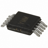
MIC2174-1YMM Micrel Inc, MIC2174-1YMM Datasheet - Page 19

MIC2174-1YMM
Manufacturer Part Number
MIC2174-1YMM
Description
IC BUCK SYNC ADJ 25A 10MSOP
Manufacturer
Micrel Inc
Series
Hyper Speed Control™r
Type
Step-Down (Buck)r
Datasheet
1.MIC2174-1YMM.pdf
(27 pages)
Specifications of MIC2174-1YMM
Internal Switch(s)
No
Synchronous Rectifier
Yes
Number Of Outputs
1
Voltage - Output
0.8 ~ 5.5 V
Frequency - Switching
300kHz
Voltage - Input
3 ~ 5.5 V
Operating Temperature
-40°C ~ 125°C
Mounting Type
Surface Mount
Package / Case
10-MSOP, Micro10™, 10-uMAX, 10-uSOP
Power - Output
421mW
Primary Input Voltage
40V
No. Of Outputs
2
Output Current
25A
Voltage Regulator Case Style
MSOP
No. Of Pins
10
Operating Temperature Range
-40°C To +125°C
Svhc
No SVHC (15-Dec-2010)
Lead Free Status / RoHS Status
Lead free / RoHS Compliant
Current - Output
-
Lead Free Status / RoHS Status
Lead free / RoHS Compliant, Lead free / RoHS Compliant
Other names
576-3546-5
Available stocks
Company
Part Number
Manufacturer
Quantity
Price
Company:
Part Number:
MIC2174-1YMM
Manufacturer:
Micrel Inc
Quantity:
135
Micrel, Inc.
2. Inadequate ripple at the FB voltage due to the small
3. Virtually no ripple at the FB pin voltage is due to the
September 2010
ESR of the output capacitors.
The output voltage ripple is fed into the FB pin
through a feedforward capacitor C
as shown in Figure 7b. The typical C
between 1nF and 100nF. With the feedforward
capacitor, the FB voltage ripple is very close to the
output voltage ripple:
very low ESR of the output capacitors.
Figure 7b. Inadequate Ripple at FB
ΔV
Figure 7c. Invisible Ripple at FB
Figure 7a. Enough Ripple at FB
FB(pp)
≈
ESR
×
ΔI
L
(pp)
ff
in this situation,
ff
value is
(36)
19
In this situation, the output voltage ripple is less than
20mV. Therefore, additional ripple is injected into the FB
pin from the switching node LX via a resistor R
capacitor C
is:
where
V
D = Duty Cycle
f
τ = (R1//R2//R
In the equations (37) and (38), it is assumed that the
time constant associated with C
than the switching period:
If the voltage divider resistors R1 and R2 are in the kΩ
range, a C
time constant consumption. Also, a 100nF injection
capacitor C
for a wide range of the frequencies.
The process of sizing the ripple injection resistor and
capacitors is:
Step 1. Select C
feedback pin and make sure the large time constant
assumption is satisfied. Typical choice of C
100nF if R1 and R2 are in kΩ range.
Step 2. Select R
voltage ripple. According to Equation 37:
Then the value of Rinj is obtained as:
SW
HSD
= switching frequency
ΔV
= Power stage input voltage at HSD pin
FB(pp)
ff
inj
inj
K
of 1nF to 100nF can easily satisfy the large
K
R
, as shown in Figure 7c. The injected ripple
=
is used in order to be considered as short
div
inj
div
inj
V
) × C
HSD
f
=
=
=
SW
inj
ff
(R1//R2)
R
ΔV
1
according to the expected feedback
×
inj
ff
×
to feed all output ripples into the
V
R1//R2
K
τ
HSD
FB(pp)
+
div
=
R1//R2
T
τ
×
×
×
D
<<
(
D
×
K
1
(1
f
×
SW
1
div
ff
-
(1
D)
must be much greater
×
MIC2174/MIC2174C
−
−
×
τ
D)
1)
f
SW
M9999-091310-C
1
×
τ
ff
is 1nF to
inj
and a
(37)
(38)
(39)
(40)


