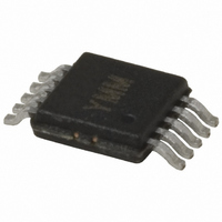
MIC2174-1YMM Micrel Inc, MIC2174-1YMM Datasheet - Page 2

MIC2174-1YMM
Manufacturer Part Number
MIC2174-1YMM
Description
IC BUCK SYNC ADJ 25A 10MSOP
Manufacturer
Micrel Inc
Series
Hyper Speed Control™r
Type
Step-Down (Buck)r
Datasheet
1.MIC2174-1YMM.pdf
(27 pages)
Specifications of MIC2174-1YMM
Internal Switch(s)
No
Synchronous Rectifier
Yes
Number Of Outputs
1
Voltage - Output
0.8 ~ 5.5 V
Frequency - Switching
300kHz
Voltage - Input
3 ~ 5.5 V
Operating Temperature
-40°C ~ 125°C
Mounting Type
Surface Mount
Package / Case
10-MSOP, Micro10™, 10-uMAX, 10-uSOP
Power - Output
421mW
Primary Input Voltage
40V
No. Of Outputs
2
Output Current
25A
Voltage Regulator Case Style
MSOP
No. Of Pins
10
Operating Temperature Range
-40°C To +125°C
Svhc
No SVHC (15-Dec-2010)
Lead Free Status / RoHS Status
Lead free / RoHS Compliant
Current - Output
-
Lead Free Status / RoHS Status
Lead free / RoHS Compliant, Lead free / RoHS Compliant
Other names
576-3546-5
Available stocks
Company
Part Number
Manufacturer
Quantity
Price
Company:
Part Number:
MIC2174-1YMM
Manufacturer:
Micrel Inc
Quantity:
135
Micrel, Inc.
Ordering Information
Pin Configuration
Pin Description
Part Number
MIC2174-1YMM
MIC2174C-1YMM
September 2010
Pin Number
1
2
3
4
5
6
7
8
Pin Name
PGND
GND
HSD
EN
DH
FB
DL
IN
Voltage
Adj.
Adj.
Pin Function
High-Side N-MOSFET Drain Connection (input): Power to the drain of the external high-side N-
channel MOSFET. The HSD operating voltage range is from 3V to 40V. Input capacitors between
HSD and the power ground (PGND) are required.
Enable (input): A logic level control of the output. The EN pin is CMOS-compatible. Logic high or
floating = enable, logic low = shutdown. In the off state, supply current of the device is greatly reduced
(typically 0.8mA).
Feedback (input): Input to the transconductance amplifier of the control loop. The FB pin is regulated
to 0.8V. A resistor divider connecting the feedback to the output is used to adjust the desired output
voltage.
Signal ground. GND is the ground path for the device input voltage V
loop for the signal ground should be separate from the power ground (PGND) loop.
Input Voltage (input): Power to the internal reference and control sections of the MIC2174/MIC2174C.
The IN operating voltage range is from 3V to 5.5V. A 2.2µF ceramic capacitors from IN to GND are
recommended for clean operation. V
function behavior correctly.
Low-Side Drive (output): High-current driver output for external low-side MOSFET. The DL driving
voltage swings from ground to IN.
Power Ground. PGND is the ground path for the MIC2174/MIC2174C buck converter power stage.
The PGND pin connects to the sources of low-side N-Channel MOSFETs, the negative terminals of
input capacitors, and the negative terminals of output capacitors. The loop for the power ground
should be as small as possible and separate from the Signal ground (GND) loop.
High-Side Drive (output): High-current driver output for external high-side MOSFET. The DH driving
voltage is floating on the switch node voltage (LX). It swings from ground to V
Adding a small resistor between DH pin and the gate of the high-side N-channel MOSFETs can slow
down the turn-on and turn-off time of the MOSFETs.
Accuracy
±1%
±3%
Switching Frequency
300kHz
270kHz
10-Pin MSOP (MM)
IN
2
must be powered up no earlier than V
Junction Temperature
–40° to +125°C
–40° to +125°C
Range
IN
and the control circuitry. The
10-Pin MSOP
10-Pin MSOP
Package
HSD
IN
MIC2174/MIC2174C
minus the diode drop.
to make the soft-start
M9999-091310-C
Lead Finish
Pb-Free
Pb-Free


