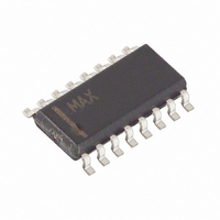
MAX1639ESE+ Maxim Integrated Products, MAX1639ESE+ Datasheet - Page 10

MAX1639ESE+
Manufacturer Part Number
MAX1639ESE+
Description
IC STEP-DWN CTRLR HI-SPD 16-SOIC
Manufacturer
Maxim Integrated Products
Type
Step-Down (Buck)r
Datasheet
1.MAX1639ESE.pdf
(13 pages)
Specifications of MAX1639ESE+
Internal Switch(s)
No
Synchronous Rectifier
Yes
Number Of Outputs
1
Voltage - Output
1.1 ~ 4.5 V
Current - Output
35A
Frequency - Switching
300kHz, 600kHz, 1MHz
Voltage - Input
4.5 ~ 5.5 V
Operating Temperature
-40°C ~ 85°C
Mounting Type
Surface Mount
Package / Case
16-SOIC (3.9mm Width)
Power - Output
696mW
Output Voltage
1.1 V to 4.5 V
Output Current
35 A
Input Voltage
4.5 V to 5.5 V
Mounting Style
SMD/SMT
Maximum Operating Temperature
+ 85 C
Minimum Operating Temperature
- 40 C
Lead Free Status / RoHS Status
Lead free / RoHS Compliant
High-Speed Step-Down Controller with
Synchronous Rectification for CPU Power
When the output exceeds the set voltage, the synchro-
nous rectifier output (DL) is driven high (and DH is dri-
ven low). This causes the inductor to quickly dissipate
any stored energy and force the fault current to flow to
ground. Current is limited by the source impedance
and parasitic resistance of the current path, so a fuse is
required in series with the +5V input to protect against
low-impedance faults, such as a shorted high-side
MOSFET. Otherwise, the low-side MOSFET will eventu-
ally fail. DL will go low if the input voltage drops below
the undervoltage lockout point.
Soft-start allows a gradual increase of the internal cur-
rent limit at start-up to reduce input surge currents. An
internal DAC raises the current-limit threshold from 0V
to 100mV in four steps (25mV, 50mV, 75mV, and
100mV) over the span of 1536 oscillator cycles.
Set the output voltage by connecting R7 and R8 (Figure 6)
to the FB pin from the output to AGND. R7 is given by the
following equation:
where V
has a maximum value of ±0.1µA, values up to 10kΩ
can be used for R8 with no significant accuracy loss.
Values under 1kΩ are recommended to improve noise
immunity. Place R7 and R8 very close to the MAX1639,
within 0.2in (5mm) of the FB pin.
An optional compensation capacitor (C8), typically
220pF, may be needed across the upper feedback
resistor to counter the effects of stray capacitance on the
FB pin, and to help ensure stable operation when high-
value feedback resistors are used (Figure 6). Empirically
adjust the feed-forward capacitor as needed.
Three key inductor parameters must be specified:
inductance value (L), peak current (I
resistance (R
constant LIR, which is the ratio of inductor peak-to-
peak AC current to DC load current. Typically LIR can
be between 0.1 to 0.5. A higher LIR value allows for
smaller inductors and better transient response, but
10
__________________Design Procedure
______________________________________________________________________________________
FB
= 1.1V. Since the input bias current at FB
DC
R
7
). The following equation includes a
Feed-Forward Compensation
=
Setting the Output Voltage
R
8
Specifying the Inductor
Overvoltage Protection
x
V
V
OUT
FB
Internal Soft-Start
−
1
PEAK
), and DC
results in higher losses and output ripple. A good com-
promise between size and loss is a 30% ripple current
to load current ratio (LIR = 0.30), which corresponds to
a peak inductor current 1.15 times higher than the DC
load current.
Figure 6. Output Selection
Figure 5. High-Side Current Sense
0.1µF
C5
MAX1639
10µF
C6
AGND
MAX1639
FB
V
CC
CSH
CSL
PLACE VERY CLOSE
TO MAX1639
R8
C8 (OPTIONAL)
R7
C10
4.7nF
10Ω
R5
C9
4.7nF
39Ω
39Ω
R10
R9
LOAD
V
OUT
N1
R1
V
C1
IN


