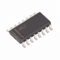
MAX1639ESE+ Maxim Integrated Products, MAX1639ESE+ Datasheet - Page 5

MAX1639ESE+
Manufacturer Part Number
MAX1639ESE+
Description
IC STEP-DWN CTRLR HI-SPD 16-SOIC
Manufacturer
Maxim Integrated Products
Type
Step-Down (Buck)r
Datasheet
1.MAX1639ESE.pdf
(13 pages)
Specifications of MAX1639ESE+
Internal Switch(s)
No
Synchronous Rectifier
Yes
Number Of Outputs
1
Voltage - Output
1.1 ~ 4.5 V
Current - Output
35A
Frequency - Switching
300kHz, 600kHz, 1MHz
Voltage - Input
4.5 ~ 5.5 V
Operating Temperature
-40°C ~ 85°C
Mounting Type
Surface Mount
Package / Case
16-SOIC (3.9mm Width)
Power - Output
696mW
Output Voltage
1.1 V to 4.5 V
Output Current
35 A
Input Voltage
4.5 V to 5.5 V
Mounting Style
SMD/SMT
Maximum Operating Temperature
+ 85 C
Minimum Operating Temperature
- 40 C
Lead Free Status / RoHS Status
Lead free / RoHS Compliant
______________________________________________________________Pin Description
PIN
10
11
12
13
14
15
16
1
2
3
4
5
6
7
8
9
PWROK
NAME
AGND
PGND
Synchronous Rectification for CPU Power
FREQ
CSH
CSL
CC1
CC2
BST
V
REF
V
DH
FB
DL
LX
CC
DD
_______________________________________________________________________________________
High-Speed Step-Down Controller with
Boost-Capacitor Bypass for High-Side MOSFET Gate Drive. Connect a 0.1µF capacitor and low-leak-
age Schottky diode as a bootstrapped charge-pump circuit to derive a 5V gate drive from V
Open-Drain Logic Output. PWROK is high when the voltage on FB is within +8% and -6% of its set-
point.
Current-Sense Amplifier’s Inverting Input. Place the current-sense resistor very close to the controller IC,
and use a Kelvin connection.
Current-Sense Amplifier’s Noninverting Input
Analog Supply Input, 5V. Use an RC filter network, as shown in Figure 1.
Reference Output, 3.5V. Bypass REF to AGND with 0.1µF (min). Sources up to 100µA for external
loads. Force REF below 2V to turn off the controller.
Analog Ground
Voltage-Feedback Input. The voltage at this input is regulated to 1.100V.
Fast-Loop Compensation Capacitor Input. Connect a ceramic capacitor and resistor in series from
CC1 to AGND. See the section Compensating the Feedback Loop.
Slow-Loop Compensation Capacitor Input. Connect a ceramic capacitor from CC2 to AGND. See the
section Compensating the Feedback Loop.
Frequency-Select Input. FREQ = V
Power Input for MOSFET Drivers, 5V. Bypass V
0.1µF capacitor and 4.7µF capacitor connected in parallel.
Low-Side Synchronous Rectifier Gate-Drive Output. DL swings between PGND and V
section BST High-Side Gate-Driver Supply and MOSFET Drivers.
Power Ground
Switching Node. Connect LX to the high-side MOSFET source and inductor.
High-Side Main MOSFET Switch Gate-Drive Output. DH is a floating driver output that swings from LX
to BST, riding on the LX switching-node voltage. See the section BST High-Side Gate-Driver Supply
and MOSFET Drivers.
FREQ = REF: 600kHz
FREQ = AGND: 300kHz
CC
: 1MHz
FUNCTION
DD
to PGND within 0.2 in. (5mm) of the V
DD
DD
. See the
pin using a
DD
for DH.
5


