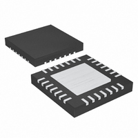
MAX5073ETI+ Maxim Integrated Products, MAX5073ETI+ Datasheet - Page 15

MAX5073ETI+
Manufacturer Part Number
MAX5073ETI+
Description
IC CONV BUCK/BOOST 28-TQFN
Manufacturer
Maxim Integrated Products
Type
Step-Down (Buck), Step-Up (Boost)r
Datasheet
1.MAX5073ETI.pdf
(25 pages)
Specifications of MAX5073ETI+
Internal Switch(s)
Yes
Synchronous Rectifier
No
Number Of Outputs
2
Voltage - Output
0.8 ~ 28 V
Current - Output
1A, 2A
Frequency - Switching
200kHz ~ 2.2MHz
Voltage - Input
4.5 ~ 23 V
Operating Temperature
-40°C ~ 85°C
Mounting Type
Surface Mount
Package / Case
28-TQFN Exposed Pad
Power - Output
2.76W
Lead Free Status / RoHS Status
Lead free / RoHS Compliant
The controller generates the clock signal by dividing
down the internal oscillator or the SYNC input signal when
driven by an external oscillator. The switching frequency
equals half the oscillator frequency (f
internal oscillator frequency is set by a resistor (R
connected from OSC to SGND. The relationship
between f
where f
For example, a 1250kHz switching frequency is set with
R
lower inductor values and less output capacitance.
Consequently, peak currents and I
at higher switching frequencies, but core losses, gate-
charge currents, and switching losses increase.
A rising clock edge on SYNC is interpreted as a syn-
chronization input. If the SYNC signal is lost, the inter-
nal oscillator takes control of the switching rate,
returning the switching frequency to that set by R
This maintains output regulation even with intermittent
SYNC signals. When an external synchronization signal
is used, R
to be lower than or equal to the SYNC rate (f
Although the MAX5073 converters can operate from
input supplies ranging from 5.5V to 23V, the input volt-
age range can be effectively limited by the MAX5073
duty-cycle limitations for a given output voltage. The
maximum input voltage is limited by the minimum on-
time (t
where t
limited by the maximum duty cycle (DMAX = 0.88):
OSC
V
2.2MHz, Dual-Output Buck or Boost Converter
IN MIN
ON(MIN)
= 10kΩ. Higher frequencies allow designs with
(
SW
ON(MIN)
SW
OSC
and f
)
=
Setting the Switching Frequency
and R
V
):
⎡
⎢
⎣
IN MAX
should be set for the oscillator frequency
V
Applications Information
is 100ns. The minimum input voltage is
OSC
(
R
OUT
OSC
______________________________________________________________________________________
OSC
0 88
)
are in hertz, and R
+
.
≤
V
=
DROP
Effective Input Voltage Range
is:
t
12.5
ON MIN
(
f
1
SW
V
×
⎤
⎥ +
⎦
OUT
)
10
V
×
DROP
9
2
Buck Converter
SW
R losses are lower
f
SW
2
= f
OSC
−
OSC
V
with Internal Power MOSFETs
SYNC
DROP
is in ohms.
/ 2). The
).
1
OSC
OSC
)
.
where V
inductor discharge path, which includes the forward
voltage drop (V
the inductor, and the PC board resistance. V
the total resistance in the charging path, which includes
the on-resistance of the high-side switch, the series
resistance of the inductor, and the PC board resistance.
For 0.8V or greater output voltages, connect a voltage-
divider from OUT_ to FB_ to SGND (Figure 5). Select
R
Calculate R
equation:
where V
table) and V
operation).
For output voltages below 0.8V, set the MAX5073 out-
put voltage by connecting a voltage-divider from the
output to FB_ to BYPASS (Figure 5). Select R
BYPASS resistor) higher than a 50kΩ range. Calculate
R
where V
Characteristics table), and V
to V
Figure 5. Adjustable Output Voltage
B
A
with the following equation:
(FB_ to SGND resistor) to between 1kΩ and 10kΩ.
FB_
MAX5073
.
DROP1
FB_
FB
LX_
FB_
V
OUT_
A
= 0.8V, V
= 0.8V (see the Electrical Characteristics
OUT_
(OUT_ to FB_ resistor) with the following
> 0.8V
R
D
is the total parasitic voltage drops in the
A
R
) of the rectifier, the series resistance of
A
=
can range from V
R
R
=
R
A
B
C
R
BYPASS
B
⎡
⎢
⎢
⎣
V
⎡
⎢
⎢
⎣
BYPASS
⎛
⎜
⎝
V
Setting the Output Voltage
V
FB
V
OUT
MAX5073
FB
OUT_
= 2V (see the Electrical
−
V
BYPASS
⎞
⎟
⎠
OUT
−
−
FB_
LX_
V
V
can range from 0V
1
OUT_
FB
⎤
⎥
⎥
⎦
FB_
< 0.8V
⎤
⎥
⎥
⎦
to 28V (boost
R
R
C
A
DROP2
C
(FB to
15
is


