MAX5082ATE+ Maxim Integrated Products, MAX5082ATE+ Datasheet - Page 14
MAX5082ATE+
Manufacturer Part Number
MAX5082ATE+
Description
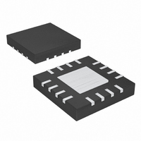
IC DC-DC CONV 1.5A 16-TQFN
Manufacturer
Maxim Integrated Products
Type
Step-Down (Buck)r
Datasheet
1.MAX5082ATE.pdf
(18 pages)
Specifications of MAX5082ATE+
Internal Switch(s)
Yes
Synchronous Rectifier
No
Number Of Outputs
1
Voltage - Output
1.23 ~ 32 V
Current - Output
1.5A
Frequency - Switching
250kHz
Voltage - Input
4.5 ~ 40 V
Operating Temperature
-40°C ~ 125°C
Mounting Type
Surface Mount
Package / Case
16-TQFN Exposed Pad
Power - Output
2.67W
Lead Free Status / RoHS Status
Lead free / RoHS Compliant


1.5A, 40V, MAXPower Step-Down
DC-DC Converters
Figure 4. Error Amplifier Compensation Circuit (Closed-Loop
and Error Amplifier Gain Plot) for Higher ESR Output Capacitors
Since R3 >> R6, R3 + R6 can be approximated as R3.
R3 is then calculated as:
f
The MAX5082/MAX5083 is available in a thermally
enhanced package and can dissipate up to 2.7W at T
+70°C. When the die temperature reaches +160°C, the
part shuts down and is allowed to cool. After the part
cools by 20°C, the device restarts with a soft-start.
14
P3
GAIN
(dB)
is set at 5xf
______________________________________________________________________________________
V
OUT
C6
C
C
8
R3
. Therefore, C8 is calculated as:
=
R
R4
R6
f
Z1
3
(
2
≈
f
π
Z2
×
2
REF
CLOSED-LOOP
GAIN
π
C
×
7
×
f
LC
C
R5
1
f
P2
EA
7
R
C8
Power Dissipation
5
×
×
f
C
C
C7
f
6
P3
f
P3
−
1
)
FREQUENCY
COMP
EA
GAIN
A
=
The power dissipated in the device is the sum of the
power dissipated from supply current (P
losses due to switching the internal power MOSFET
(P
rent through the internal power MOSFET (P
The total power dissipated in the package must be lim-
ited such that the junction temperature does not
exceed its absolute maximum rating of +150°C at maxi-
mum ambient temperature. Calculate the power lost in
the MAX5082/MAX5083 using the following equations:
The power loss through the switch:
R
(see the Electrical Characteristics).
The power loss due to switching the internal MOSFET:
where t
power MOSFET measured at LX.
The power loss due to the switching supply current
(I
The total power dissipated in the device will be:
TRANSISTOR COUNT: 4300
PROCESS: BiCMOS/DMOS
SW
ON
SW
I
RMS MOSFET
):
), and the power dissipated due to the RMS cur-
is the on-resistance of the internal power MOSFET
R
_
and t
P
P
MOSFET
P
SW
P
MOSFET
TOTAL
F
=
are the rise and fall times of the internal
I
I
PK
DC
=
V
IN
=
= P
P
=
[
=
= I
I
I
RMS MOSFET
Q
2
×
I
I
PK
OUT
OUT
MOSFET
RMS_MOSFET
= V
I
OUT
_
+
(
IN
+
−
I
PK
Chip Information
×
∆
∆
x I
4
I
I
(
P P
P P
×
+ P
2
2
t
SW
R
−
−
I
DC
2
×
SW
t
×
2
)
F
R
+
x R
)
+ P
ON
I
×
2
DC
ON
f
SW
Q
Q
), transition
]
×
MOSFET
D
3
).
Related parts for MAX5082ATE+
Image
Part Number
Description
Manufacturer
Datasheet
Request
R

Part Number:
Description:
1.5A, 40V, MAXPower Step-Down DC-DC Converters
Manufacturer:
MAXIM [Maxim Integrated Products]
Datasheet:
Part Number:
Description:
Voltage-Output, 12-Bit DACs with Internal Reference
Manufacturer:
MAXIM [Maxim Integrated Products]
Datasheet:

Part Number:
Description:
MAX7528KCWPMaxim Integrated Products [CMOS Dual 8-Bit Buffered Multiplying DACs]
Manufacturer:
Maxim Integrated Products
Datasheet:
Part Number:
Description:
Single +5V, fully integrated, 1.25Gbps laser diode driver.
Manufacturer:
Maxim Integrated Products
Datasheet:
Part Number:
Description:
Single +5V, fully integrated, 155Mbps laser diode driver.
Manufacturer:
Maxim Integrated Products
Datasheet:
Part Number:
Description:
VRD11/VRD10, K8 Rev F 2/3/4-Phase PWM Controllers with Integrated Dual MOSFET Drivers
Manufacturer:
Maxim Integrated Products
Datasheet:
Part Number:
Description:
Highly Integrated Level 2 SMBus Battery Chargers
Manufacturer:
Maxim Integrated Products
Datasheet:
Part Number:
Description:
Current Monitor and Accumulator with Integrated Sense Resistor; ; Temperature Range: -40°C to +85°C
Manufacturer:
Maxim Integrated Products
Part Number:
Description:
TSSOP 14/A°/RS-485 Transceivers with Integrated 100O/120O Termination Resis
Manufacturer:
Maxim Integrated Products
Part Number:
Description:
TSSOP 14/A°/RS-485 Transceivers with Integrated 100O/120O Termination Resis
Manufacturer:
Maxim Integrated Products
Part Number:
Description:
QFN 16/A°/AC-DC and DC-DC Peak-Current-Mode Converters with Integrated Step
Manufacturer:
Maxim Integrated Products
Part Number:
Description:
TDFN/A/65V, 1A, 600KHZ, SYNCHRONOUS STEP-DOWN REGULATOR WITH INTEGRATED SWI
Manufacturer:
Maxim Integrated Products
Part Number:
Description:
Integrated Temperature Controller f
Manufacturer:
Maxim Integrated Products
Part Number:
Description:
SOT23-6/I°/45MHz to 650MHz, Integrated IF VCOs with Differential Output
Manufacturer:
Maxim Integrated Products
Part Number:
Description:
SOT23-6/I°/45MHz to 650MHz, Integrated IF VCOs with Differential Output
Manufacturer:
Maxim Integrated Products