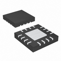
MAX5082ATE+ Maxim Integrated Products, MAX5082ATE+ Datasheet - Page 9

MAX5082ATE+
Manufacturer Part Number
MAX5082ATE+
Description
IC DC-DC CONV 1.5A 16-TQFN
Manufacturer
Maxim Integrated Products
Type
Step-Down (Buck)r
Datasheet
1.MAX5082ATE.pdf
(18 pages)
Specifications of MAX5082ATE+
Internal Switch(s)
Yes
Synchronous Rectifier
No
Number Of Outputs
1
Voltage - Output
1.23 ~ 32 V
Current - Output
1.5A
Frequency - Switching
250kHz
Voltage - Input
4.5 ~ 40 V
Operating Temperature
-40°C ~ 125°C
Mounting Type
Surface Mount
Package / Case
16-TQFN Exposed Pad
Power - Output
2.67W
Lead Free Status / RoHS Status
Lead free / RoHS Compliant
SS is the 1.23V reference bypass connection for the
MAX5082/MAX5083 and also controls the soft-start
period. At startup, after V
and external UVLO thresholds are reached, the device
enters soft-start. During soft-start, 15µA is sourced into
the capacitor (C
ing the reference voltage to ramp up slowly. When V
reaches 1.23V the output becomes fully active. Set the
soft-start time (t
where t
Figure 2. MAX5083 Simplified Block Diagram
COMP
SYNC
REG
SS
FB
SS
I
SS
is in seconds and C
OSC
IN
EN
SS
1.23V
SS
Soft-Start and Reference (SS)
) using the following equation:
t
_______________________________________________________________________________________
) connected from SS to SGND caus-
SS
LDO
EN
REF
=
1 23
RAMP
.
IN
IN
E/A
V
15
REF
V
is applied and the internal
SS
×
µ
A
1.23V
C
0.3V
is in Farads.
SS
1.5A, 40V, MAXPower Step-Down
THERMAL
SHDN
CPWM
1.23V
CLK
<1.11V OFF
>1.23V ON
ON/OFF
SS
REGOK
SSA
The MAX5082 features an internal charge pump to
enhance the turn-on of the internal MOSFET, allowing
for operation with input voltages down to 4.5V. Connect
a flying capacitor (C
diode from C+ to BST, as well as a bootstrap capacitor
(C
voltage for the high-side n-channel DMOS switch.
During the on-time, the flying capacitor is charged to
V
flying capacitor (C+) is pumped to two times V
and charge is dumped onto C
regulator voltage across the high-side DMOS driver.
Use a ceramic capacitor of at least 0.1µF for C
C
For applications that do not require a 4.5V minimum
input, use the MAX5083. In this device, the charge
DVREG
F
BST
located as close to the device as possible.
V
REF
) between BST and LX to provide the gate-drive
EN
. During the off-time, the positive terminal of the
ILIM
OVERL
DC-DC Converters
Internal Charge Pump (MAX5082)
BOOTSTRAP
CONTROL
PFM
MANAGEMENT
ILIM
LOGIC
OVERLOAD
F
) between C+ and C-, a boost
PCLK
SCLK
REF_ILIM
REF_PFM
MAX5083
ILIM
CLK
BST
to provide twice the
HIGH-SIDE
CURRENT
SENSE
BST
DVREG
SGND
IN
BST
LX
DVREG
PGND
and
9


