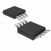
LTC3200EMS8 Linear Technology, LTC3200EMS8 Datasheet - Page 6

LTC3200EMS8
Manufacturer Part Number
LTC3200EMS8
Description
IC SW CAP/DBLR .1A 8MSOP
Manufacturer
Linear Technology
Type
Switched Capacitor (Charge Pump), Doublerr
Datasheet
1.LTC3200ES6-5TRMPBF.pdf
(12 pages)
Specifications of LTC3200EMS8
Internal Switch(s)
Yes
Synchronous Rectifier
No
Number Of Outputs
1
Current - Output
100mA
Frequency - Switching
2MHz
Voltage - Input
2.7 ~ 4.5 V
Operating Temperature
-40°C ~ 85°C
Mounting Type
Surface Mount
Package / Case
8-MSOP, Micro8™, 8-uMAX, 8-uSOP,
Lead Free Status / RoHS Status
Contains lead / RoHS non-compliant
Voltage - Output
-
Power - Output
-
Available stocks
Company
Part Number
Manufacturer
Quantity
Price
Company:
Part Number:
LTC3200EMS8
Manufacturer:
LT
Quantity:
10 000
Part Number:
LTC3200EMS8
Manufacturer:
LINEAR/凌特
Quantity:
20 000
Part Number:
LTC3200EMS8#PBF
Manufacturer:
ADI/亚德诺
Quantity:
20 000
Company:
Part Number:
LTC3200EMS8#TRPBF
Manufacturer:
MT
Quantity:
6 218
LTC3200/LTC3200-5
Operation (Refer to Simplified Block Diagrams)
The LTC3200/LTC3200-5 use a switched capacitor charge
pump to boost V
tion is achieved by sensing the output voltage through an
internal resistor divider (LTC3200-5) and modulating the
charge pump output current based on the error signal. A
2-phase nonoverlapping clock activates the charge pump
switches. The flying capacitor is charged from V
first phase of the clock. On the second phase of the clock
it is stacked in series with V
sequence of charging and discharging the flying capacitor
continues at a free running frequency of 2MHz (typ).
In shutdown mode all circuitry is turned off and the
LTC3200/LTC3200-5 draw only leakage current from the
V
The SHDN pin is a CMOS input with a threshold voltage of
approximately 0.8V. The LTC3200/LTC3200-5 is in shut-
down when a logic low is applied to the SHDN pin. Since
the SHDN pin is a high impedance CMOS input it should
never be allowed to float. To ensure that its state is defined
it must always be driven with a valid logic level.
Short-Circuit/Thermal Protection
The LTC3200/LTC3200-5 have built-in short-circuit current
limiting as well as overtemperature protection. During
short-circuit conditions, they will automatically limit their
output current to approximately 225mA. At higher tempera-
tures, or if the input voltage is high enough to cause exces-
sive self heating on chip, thermal shutdown circuitry will
shut down the charge pump once the junction temperature
exceeds approximately 160 C. It will reenable the charge
pump once the junction temperature drops back to approxi-
mately 155 C. The LTC3200/LTC3200-5 will cycle in and
out of thermal shutdown indefinitely without latch-up or
damage until the short-circuit on V
Shutdown Current
Since the output voltage can go above the input voltage,
special circuitry is required to control internal logic.
Detection logic will draw an input current of 5 A when the
LTC3200 is in shutdown. However, this current will be
eliminated when the output voltage (V
6
OPERATIO
IN
supply. Furthermore, V
IN
U
to a regulated output voltage. Regula-
IN
OUT
and connected to V
is disconnected from V
OUT
is removed.
OUT
) is at 0V. To
OUT
IN
on the
. This
IN
.
ensure that V
LTC3200 a bleed resistor may be needed from V
Typically 10k to 100k is acceptable.
Soft-Start
The LTC3200/LTC3200-5 have built-in soft-start circuitry
to prevent excessive current flow at V
The soft-start time is preprogrammed to approximately
1ms, so the start-up current will be primarily dependent
upon the output capacitor. The start-up input current can
be calculated with the expression:
For example, with a 2.2 F output capacitor the start-up
input current of an LTC3200-5 will be approximately
22mA. If the output capacitor is 10 F then the start-up
input current will be about 100mA.
Programming the LTC3200 Output Voltage (FB Pin)
While the LTC3200-5 version has an internal resistive
divider to program the output voltage, the programmable
LTC3200 may be set to an arbitrary voltage via an external
resistive divider. Since it employs a voltage doubling
charge pump, it is not possible to achieve output voltages
greater than twice the available input voltage. Figure 1
shows the required voltage divider connection.
The voltage divider ratio is given by the expression:
Typical values for total voltage divider resistance can
range from several k s up to 1M .
I
R
R
STARTUP
2
1
Figure 1. Programming the Adjustable LTC3200
1 268
V
.
OUT
OUT
2
V
C
PGND
SGND
V
–
OUT
is at 0V in shutdown on the adjustable
OUT
FB
1
8
7
4
5
V
1
OUT
ms
R1
R2
32005 F01
C
OUT
V
1.268V 1 + R1
OUT
IN
during start-up.
R2
OUT
to GND.


