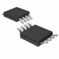
LTC3200EMS8 Linear Technology, LTC3200EMS8 Datasheet - Page 9

LTC3200EMS8
Manufacturer Part Number
LTC3200EMS8
Description
IC SW CAP/DBLR .1A 8MSOP
Manufacturer
Linear Technology
Type
Switched Capacitor (Charge Pump), Doublerr
Datasheet
1.LTC3200ES6-5TRMPBF.pdf
(12 pages)
Specifications of LTC3200EMS8
Internal Switch(s)
Yes
Synchronous Rectifier
No
Number Of Outputs
1
Current - Output
100mA
Frequency - Switching
2MHz
Voltage - Input
2.7 ~ 4.5 V
Operating Temperature
-40°C ~ 85°C
Mounting Type
Surface Mount
Package / Case
8-MSOP, Micro8™, 8-uMAX, 8-uSOP,
Lead Free Status / RoHS Status
Contains lead / RoHS non-compliant
Voltage - Output
-
Power - Output
-
Available stocks
Company
Part Number
Manufacturer
Quantity
Price
Company:
Part Number:
LTC3200EMS8
Manufacturer:
LT
Quantity:
10 000
Part Number:
LTC3200EMS8
Manufacturer:
LINEAR/凌特
Quantity:
20 000
Part Number:
LTC3200EMS8#PBF
Manufacturer:
ADI/亚德诺
Quantity:
20 000
Company:
Part Number:
LTC3200EMS8#TRPBF
Manufacturer:
MT
Quantity:
6 218
OPERATIO
Power Efficiency
The power efficiency ( ) of the LTC3200/LTC3200-5 is
similar to that of a linear regulator with an effective input
voltage of twice the actual input voltage. This occurs
because the input current for a voltage doubling charge
pump is approximately twice the output current. In an ideal
regulating voltage doubler the power efficiency would be
given by:
At moderate to high output power the switching losses
and quiescent current of the LTC3200/LTC3200-5 are
negligible and the expression above is valid. For example
with V
measured efficiency is 80% which is in close agreement
with the theoretical 83.3% calculation.
Operation at V
LTC3200/LTC3200-5 will continue to operate with input
voltages somewhat above 5V. However, because of its
constant frequency nature, some charge due to internal
switching will be coupled to V
movement of the output voltage at very light loads. To
avoid an output overvoltage problem with high V
moderate standing load current of 1mA will help the
LTC3200/LTC3200-5 maintain exceptional line regula-
tion. This can be achieved with a 5k resistor from V
GND.
IN
SHDN
V
GND
P
OUT
V
P
= 3V, I
OUT
IN
IN
1 F
Figure 5. Recommended Layout
OUT
IN
V
V
OUT
> 5V
U
IN
= 50mA and V
• 2
•
I
I
OUT
OUT
LTC3200-5
OUT
V
2
OUT
V
OUT
causing a slight upward
IN
regulating to 5V the
1 F
1 F
32005 F03
OUT
IN
, a
to
Layout Considerations
Due to its high switching frequency and the high transient
currents produced by the LTC3200/LTC3200-5, careful
board layout is necessary. A true ground plane and short
connections to all capacitors will improve performance and
ensure proper regulation under all conditions. Figure 5
shows an example layout for the LTC3200-5.
Thermal Management
For higher input voltages and maximum output current
there can be substantial power dissipation in the LTC3200/
LTC3200-5. If the junction temperature increases above
approximately 160 C the thermal shutdown circuitry will
automatically deactivate the output. To reduce the
maximum junction temperature, a good thermal connec-
tion to the PC board is recommended. Connecting the
GND pin (Pins 4/5 for LTC3200, Pin 2 for LTC3200-5) to
a ground plane, and maintaining a solid ground plane
under the device on two layers of the PC board can reduce
the thermal resistance of the package and PC board
considerably.
Derating Power at Higher Temperatures
To prevent an overtemperature condition in high power
applications Figure 6 should be used to determine the
maximum combination of ambient temperature and power
dissipation.
Figure 6. Maximum Power Dissipation
vs Ambient Temperature
1.2
1.0
0.8
0.6
0.4
0.2
0
–50
LTC3200/LTC3200-5
–25
AMBIENT TEMPERATURE ( C)
0
25
50
T
J
JA
= 160 C
= 175 C/W
75
32005 • F06
100
9


