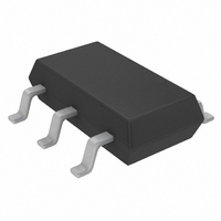
LTC3459ES6#TRPBF Linear Technology, LTC3459ES6#TRPBF Datasheet

LTC3459ES6#TRPBF
Specifications of LTC3459ES6#TRPBF
Available stocks
Related parts for LTC3459ES6#TRPBF
LTC3459ES6#TRPBF Summary of contents
Page 1
... The LTC3459 is offered in low profi le 6-pin 2mm × 2mm DFN, 2mm × 3mm DFN or SOT-23 (ThinSOT allowing a tiny footprint for the total solution. , LT, LTC, LTM and Burst Mode are registered trademarks of Linear Technology Corporation. ThinSOT is a trademark of Linear Technology Corporation. All other trademarks are the property of their respective owners. ...
Page 2
... LTC3459EDC#TRPBF LTC3459EDCB#PBF LTC3459EDCB#TRPBF LTC3459ES6#PBF LTC3459ES6#TRPBF Consult LTC Marketing for parts specifi ed with wider operating temperature ranges. Consult LTC Marketing for information on non-standard lead based fi nish parts. For more information on lead free part marking, go to: For more information on tape and reel specifi cations, go to: 2 Storage Temperature Range .................. – ...
Page 3
ELECTRICAL CHARACTERISTICS temperature range, otherwise specifi cations are at T PARAMETER V IN Input Voltage Range V Quiescent Current IN V Shutdown Current IN V OUT Programmable Voltage Range V Quiescent Supply Current OUT V Shutdown Current OUT Reference Feedback ...
Page 4
LTC3459 TYPICAL PERFORMANCE CHARACTERISTICS Minimum OUT IN 4000 V = 10V OUT V = 7.5V OUT 3500 OUT V = 3.3V OUT 3000 L = 22μH 2500 2000 1500 1000 500 0 1.5 2 ...
Page 5
TYPICAL PERFORMANCE CHARACTERISTICS V AC Ripple OUT V OUT 50mV/DIV INDUCTOR CURRENT 50mA/DIV V = 3.3V 5μs/DIV 3459 G10 OUT L = 22μ 4.7μF OUT C = 47pF FF V Regulated Below OUT V ...
Page 6
LTC3459 PIN FUNCTIONS (DC/DCB/S6 Packages) V (Pin 1/Pin 6/Pin 6): Input Supply Pin. Bypass low ESR, ESL ceramic capacitor of at least 1μ (Pin 2/Pin 2/Pin 5): Regulated Output Voltage of OUT the Boost Regulator. ...
Page 7
OPERATION Operation The LTC3459 synchronous boost converter utilizes a Burst Mode control technique to achieve high effi ciency over a wide dynamic range. A 2.5% accurate comparator is used to monitor the output voltage (V above the comparator threshold, no ...
Page 8
LTC3459 OPERATION This is accomplished by varying the t proximately 1/(V – Due to propagation delays OUT IN and a 0.6μA bias current in the timer, the t more accurately predicted as follows: APPLICATIONS INFORMATION Inductor Selection An ...
Page 9
TYPICAL APPLICATIONS Very low operating quiescent current and synchronous operation allow for greater than 85% conversion effi ciency in many applications. Lower output voltages will result in lower effi ciencies since the N- and P-channel R will increase. The switching ...
Page 10
LTC3459 TYPICAL APPLICATIONS controlled, preventing any damaging effects of inrush current. Proper heat sinking of the package is required in this application as the die may dissipate 100mW to 200mW during initial charging. When V OUT normal boost mode operation ...
Page 11
... DIMENSIONS ARE INCLUSIVE OF PLATING Information furnished by Linear Technology Corporation is believed to be accurate and reliable. However, no responsibility is assumed for its use. Linear Technology Corporation makes no representa- tion that the interconnection of its circuits as described herein will not infringe on existing patent rights. DCB Package 6-Lead Plastic DFN (2mm × ...
Page 12
... I < 1μA, MS10 OUT(MAX 5.25V 12μA, I < 1μA, OUT(MAX 5V 20μA/300μA, I < 1μA, ThinSOT OUT(MAX 5V 20μA/300μA, I < 1μA, ThinSOT OUT(MAX 34V 25μA, I < 1μA, ThinSOT OUT(MAX 1208 REV C • PRINTED IN USA © LINEAR TECHNOLOGY CORPORATION 2007 3459fc ...


