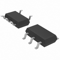
LTC3406ES5#TR Linear Technology, LTC3406ES5#TR Datasheet - Page 10

LTC3406ES5#TR
Manufacturer Part Number
LTC3406ES5#TR
Description
IC REG SYNC SDWN 1.5MHZ TSOT23-5
Manufacturer
Linear Technology
Type
Step-Down (Buck)r
Datasheet
1.LTC3406ES5TRMPBF.pdf
(16 pages)
Specifications of LTC3406ES5#TR
Internal Switch(s)
Yes
Synchronous Rectifier
Yes
Number Of Outputs
1
Voltage - Output
0.6 ~ 5.5 V
Current - Output
600mA
Frequency - Switching
1.5MHz
Voltage - Input
2.5 ~ 5.5 V
Operating Temperature
-40°C ~ 85°C
Mounting Type
Surface Mount
Package / Case
TSOT-23-5, TSOT-5, TSOP-5
Lead Free Status / RoHS Status
Contains lead / RoHS non-compliant
Power - Output
-
Other names
LTC3406ES5TR
Available stocks
Company
Part Number
Manufacturer
Quantity
Price
APPLICATIO S I FOR ATIO
LTC3406
LTC3406-1.5/LTC3406-1.8
Although all dissipative elements in the circuit produce
losses, two main sources usually account for most of the
losses in LTC3406 circuits: V
losses. The V
efficiency loss at very low load currents whereas the I
loss dominates the efficiency loss at medium to high load
currents. In a typical efficiency plot, the efficiency curve at
very low load currents can be misleading since the actual
power lost is of no consequence as illustrated in Figure 4.
1. The V
10
the DC bias current as given in the electrical character-
istics and the internal main switch and synchronous
switch gate charge currents. The gate charge current
results from switching the gate capacitance of the
internal power MOSFET switches. Each time the gate is
switched from high to low to high again, a packet of
charge, dQ, moves from V
dQ/dt is the current out of V
the DC bias current. In continuous mode, I
f(Q
internal top and bottom switches. Both the DC bias and
gate charge losses are proportional to V
their effects will be more pronounced at higher supply
voltages.
T
0.00001
+ Q
0.0001
IN
0.001
0.01
0.1
B
quiescent current is due to two components:
1
) where Q
0.1
Figure 4. Power Lost vs Load Current
IN
quiescent current loss dominates the
V
V
V
V
U
OUT
OUT
OUT
OUT
1
LOAD CURRENT (mA)
T
= 1.2V
= 1.5V
= 1.8V
= 2.5V
and Q
U
10
B
IN
IN
IN
are the gate charges of the
quiescent current and I
that is typically larger than
to ground. The resulting
100
W
3406 F04
1000
IN
U
GATECHG
and thus
2
2
R
R
=
2. I
Other losses including C
losses and inductor core losses generally account for less
than 2% total additional loss.
Thermal Considerations
In most applications the LTC3406 does not dissipate
much heat due to its high efficiency. But, in applications
where the LTC3406 is running at high ambient tempera-
ture with low supply voltage and high duty cycles, such
as in dropout, the heat dissipated may exceed the maxi-
mum junction temperature of the part. If the junction
temperature reaches approximately 150°C, both power
switches will be turned off and the SW node will become
high impedance.
To avoid the LTC3406 from exceeding the maximum
junction temperature, the user will need to do some
thermal analysis. The goal of the thermal analysis is to
determine whether the power dissipated exceeds the
maximum junction temperature of the part. The tempera-
ture rise is given by:
where P
is the thermal resistance from the junction of the die to the
ambient temperature.
internal switches, R
continuous mode, the average output current flowing
through inductor L is “chopped” between the main
switch and the synchronous switch. Thus, the series
resistance looking into the SW pin is a function of both
top and bottom MOSFET R
(DC) as follows:
The R
be obtained from the Typical Performance Charateristics
curves. Thus, to obtain I
R
output current.
T
2
R
L
R losses are calculated from the resistances of the
R
= (P
and multiply the result by the square of the average
SW
D
DS(ON)
is the power dissipated by the regulator and θ
D
= (R
)(θ
JA
DS(ON)TOP
for both the top and bottom MOSFETs can
)
SW
)(DC) + (R
, and external inductor R
IN
2
R losses, simply add R
and C
DS(ON)
DS(ON)BOT
OUT
and the duty cycle
ESR dissipative
)(1 – DC)
SW
L
3406fa
. In
to
JA


