LTC3406ES5#TR Linear Technology, LTC3406ES5#TR Datasheet - Page 6

LTC3406ES5#TR
Manufacturer Part Number
LTC3406ES5#TR
Description
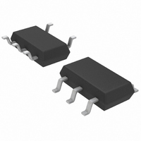
IC REG SYNC SDWN 1.5MHZ TSOT23-5
Manufacturer
Linear Technology
Type
Step-Down (Buck)r
Datasheet
1.LTC3406ES5TRMPBF.pdf
(16 pages)
Specifications of LTC3406ES5#TR
Internal Switch(s)
Yes
Synchronous Rectifier
Yes
Number Of Outputs
1
Voltage - Output
0.6 ~ 5.5 V
Current - Output
600mA
Frequency - Switching
1.5MHz
Voltage - Input
2.5 ~ 5.5 V
Operating Temperature
-40°C ~ 85°C
Mounting Type
Surface Mount
Package / Case
TSOT-23-5, TSOT-5, TSOP-5
Lead Free Status / RoHS Status
Contains lead / RoHS non-compliant
Power - Output
-
Other names
LTC3406ES5TR
Available stocks
Company
Part Number
Manufacturer
Quantity
Price
FU CTIO AL DIAGRA
OPERATIO
LTC3406
LTC3406-1.5/LTC3406-1.8
Main Control Loop
The LTC3406 uses a constant frequency, current mode
step-down architecture. Both the main (P-channel
MOSFET) and synchronous (N-channel MOSFET) switches
are internal. During normal operation, the internal top
power MOSFET is turned on each cycle when the oscillator
sets the RS latch, and turned off when the current com-
parator, I
current at which I
the output of error amplifier EA. When the load current
increases, it causes a slight decrease in the feedback
voltage, FB, relative to the 0.6V reference, which in turn,
causes the EA amplifier’s output voltage to increase until
the average inductor current matches the new load cur-
rent. While the top MOSFET is off, the bottom MOSFET is
turned on until either the inductor current starts to reverse,
as indicated by the current reversal comparator I
the beginning of the next clock cycle.
6
V
LTC3406-1.5
R1 + R2 = 550k
LTC3406-1.8
R1 + R2 = 540k
FB
RUN
U
/V
1
5
OUT
COMP
0.6V REF
U
V
IN
, resets the RS latch. The peak inductor
R1
R2
SHUTDOWN
COMP
U
(Refer to Functional Diagram)
FB
resets the RS latch, is controlled by
SHIFT
FREQ
OSC
0.6V
+
–
EA
SLOPE
COMP
W
–
+
OSC
RCMP
, or
0.4V
Burst Mode Operation
The LTC3406 is capable of Burst Mode operation in which
the internal power MOSFETs operate intermittently based
on load demand.
In Burst Mode operation, the peak current of the inductor
is set to approximately 200mA regardless of the output
load. Each burst event can last from a few cycles at light
loads to almost continuously cycling with short sleep
intervals at moderate loads. In between these burst events,
the power MOSFETs and any unneeded circuitry are turned
off, reducing the quiescent current to 20µA. In this sleep
state, the load current is being supplied solely from the
output capacitor. As the output voltage droops, the EA
amplifier’s output rises above the sleep threshold signal-
ing the BURST comparator to trip and turn the top MOSFET
on. This process repeats at a rate that is dependent on the
load demand.
RS LATCH
–
+
R
S
BURST
Q
Q
SLEEP
SWITCHING
BLANKING
CIRCUIT
LOGIC
AND
0.65V
–
I
SHOOT-
COMP
ANTI-
THRU
I
RCMP
+
+
–
5Ω
3406 BD
4
3
2
3406fa
V
SW
GND
IN


