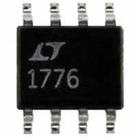
LT1776CS8 Linear Technology, LT1776CS8 Datasheet - Page 8

LT1776CS8
Manufacturer Part Number
LT1776CS8
Description
IC SW REG STEP-DOWN HI-EFF 8SOIC
Manufacturer
Linear Technology
Type
Step-Down (Buck)r
Datasheet
1.LT1776CS8PBF.pdf
(20 pages)
Specifications of LT1776CS8
Internal Switch(s)
Yes
Synchronous Rectifier
No
Number Of Outputs
1
Voltage - Output
1.24 ~ 34 V
Current - Output
700mA
Frequency - Switching
200kHz
Voltage - Input
7.4 ~ 40 V
Operating Temperature
0°C ~ 125°C
Mounting Type
Surface Mount
Package / Case
8-SOIC (3.9mm Width)
Lead Free Status / RoHS Status
Contains lead / RoHS non-compliant
Power - Output
-
Available stocks
Company
Part Number
Manufacturer
Quantity
Price
Part Number:
LT1776CS8
Manufacturer:
LINEAR/凌特
Quantity:
20 000
Part Number:
LT1776CS8#PBF
Manufacturer:
LT/凌特
Quantity:
20 000
Part Number:
LT1776CS8#TRPBF
Manufacturer:
LINEAR/凌特
Quantity:
20 000
OPERATIO
The system as previously described handles heavy loads
(continuous mode) at good efficiency, but it is actually
counterproductive for light loads. The method of jam-
ming charge into the PNP bases makes it difficult to turn
them off rapidly and achieve the very short switch ON
times required by light loads in discontinuous mode.
Furthermore, the high leading edge dV/dt rate similarly
adversely affects light load controllability.
The solution is to employ a “boost comparator” whose
inputs are the V
threshold reference, V
mode switching topology, the V
peak switch current.) When the V
previously described “high dV/dt” action is performed.
When the V
absent, as can be seen in the Low dV/dt Mode Timing
Diagram. Now the DC current, activated by the SWON
APPLICATIONS
LT1776
Selecting a Power Inductor
There are several parameters to consider when selecting
a power inductor. These include inductance value, peak
current rating (to avoid core saturation), DC resistance,
construction type, physical size, and of course, cost.
In a typical application, proper inductance value is dictated
by matching the discontinuous/continuous crossover point
with the LT1776 internal low-to-high dV/dt threshold. This
is the best compromise between maintaining control with
light loads while maintaining good efficiency with heavy
loads. The fixed internal dV/dt threshold has a nominal
value of 1.4V, which referred to the V
control voltage to switch transconductance, corresponds
to a peak current of about 200mA. Standard buck con-
verter theory yields the following expression for induc-
tance at the discontinuous/continuous crossover:
8
L
f I
V
•
OUT
PK
C
signal is below V
C
V
U
IN
control voltage and a fixed internal
U
–
V
IN
TH
V
OUT
INFORMATION
. (Remember that in a current
U
TH
C
C
voltage determines the
signal is above V
, the boost pulses are
W
C
pin threshold and
U
TH
, the
signal alone, drives Q4 and this transistor drives Q1 by
itself. The absence of a boost pulse, plus the lack of a
second NPN driver, result in a much lower slew rate which
aids light load controllability.
A further aid to overall efficiency is provided by the
specialized bias regulator circuit, which has a pair of
inputs, V
the switching supply output. During start-up conditions,
the LT1776 powers itself directly from V
the switching supply output voltage reaches about 2.9V,
the bias regulator uses this supply as its input. Previous
generation buck controller ICs without this provision
typically required hundreds of milliwatts of quiescent
power when operating at high input voltage. This both
degraded efficiency and limited available output current
due to internal heating.
For example, substituting 40V, 5V, 200mA and 200kHz
respectively for V
100 H. Note that the left half of this expression is indepen-
dent of input voltage while the right half is only a weak
function of V
means that a single inductor value will work well over a
range of “high” input voltage. And although a progres-
sively smaller inductor is suggested as V
approach V
under these conditions are much more forgiving with
respect to controllability and efficiency issues. Therefore
when a wide input voltage range must be accommodated,
say 10V to 40V for 5V
inductance value based on the maximum input voltage.
Once the inductance value is decided, inductor peak
current rating and resistance need to be considered. Here,
the inductor peak current rating refers to the onset of
saturation in the core material, although manufacturers
sometimes specify a “peak current rating” which is de-
rived from a worst-case combination of core saturation
and self-heating effects. Inductor winding resistance alone
IN
and V
OUT
IN
, note that the much higher ON duty cycles
when V
CC
IN
, V
. The V
OUT
IN
OUT
, I
is much greater than V
CC
PK
, the user should choose an
pin is normally connected to
and f yields a value of about
IN
. However, after
IN
begins to
OUT
. This


