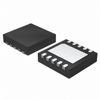
LTC3411EDD Linear Technology, LTC3411EDD Datasheet - Page 14

LTC3411EDD
Manufacturer Part Number
LTC3411EDD
Description
IC DC/DC CONV STEP-DOWN 10DFN
Manufacturer
Linear Technology
Type
Step-Down (Buck)r
Datasheet
1.LTC3411EDDPBF.pdf
(24 pages)
Specifications of LTC3411EDD
Internal Switch(s)
Yes
Synchronous Rectifier
Yes
Number Of Outputs
1
Voltage - Output
0.8 ~ 5 V
Current - Output
1.25A
Frequency - Switching
1MHz
Voltage - Input
2.63 ~ 5.5 V
Operating Temperature
-40°C ~ 85°C
Mounting Type
Surface Mount
Package / Case
10-DFN
Lead Free Status / RoHS Status
Contains lead / RoHS non-compliant
Power - Output
-
Available stocks
Company
Part Number
Manufacturer
Quantity
Price
Company:
Part Number:
LTC3411EDD
Manufacturer:
LT
Quantity:
10 000
Part Number:
LTC3411EDD
Manufacturer:
LT/凌特
Quantity:
20 000
Part Number:
LTC3411EDD#PBF
Manufacturer:
LINEAR/凌特
Quantity:
20 000
Company:
Part Number:
LTC3411EDD#TRPBF
Manufacturer:
PANASONIC
Quantity:
23 000
Part Number:
LTC3411EDD#TRPBF
Manufacturer:
LT
Quantity:
20 000
APPLICATIONS INFORMATION
LTC3411
overshoot seen at this pin. The bandwidth can also be
estimated by examining the rise time at the pin.
The I
will provide an adequate starting point for most applica-
tions. The series R-C fi lter sets the dominant pole-zero
loop compensation. The values can be modifi ed slightly
(from 0.5 to 2 times their suggested values) to optimize
transient response once the fi nal PC layout is done and
the particular output capacitor type and value have been
determined. The output capacitors need to be selected
because the various types and values determine the loop
feedback factor gain and phase. An output current pulse of
20% to 100% of full load current having a rise time of 1μs
to 10μs will produce output voltage and I
that will give a sense of the overall loop stability without
breaking the feedback loop.
Switching regulators take several cycles to respond to a
step in load current. When a load step occurs, V
mediately shifts by an amount equal to ΔI
ESR is the effective series resistance of C
begins to charge or discharge C
error signal used by the regulator to return V
steady-state value. During this recovery time, V
be monitored for overshoot or ringing that would indicate
a stability problem.
14
TH
external components shown in the Figure 1 circuit
TO 5.5V
2.5V
V
IN
SGND
PGND
C6
C
ITH
OUT
+
PGND
SGND
generating a feedback
C
IN
C8
C
C
R
SGND
C
SGND
LOAD
TH
OUT
R6
pin waveforms
Figure 5. LTC3411 General Schematic
. ΔI
• ESR, where
SV
SYNC/MODE
I
SGND PGND
TH
IN
OUT
LOAD
OUT
OUT
GND
LTC3411
PV
to its
also
IN
can
im-
SHDN/R
PGOOD
SW
V
FB
T
The initial output voltage step may not be within the
bandwidth of the feedback loop, so the standard second
order overshoot/DC ratio cannot be used to determine
phase margin. The gain of the loop increases with R and
the bandwidth of the loop increases with decreasing C.
If R is increased by the same factor that C is decreased,
the zero frequency will be kept the same, thereby keeping
the phase the same in the most critical frequency range
of the feedback loop. In addition, a feedforward capacitor
C
as shown in Figure 5. Capacitor C
creating a high frequency zero with R2 which improves
the phase margin.
The output voltage settling behavior is related to the stability
of the closed-loop system and will demonstrate the actual
overall supply performance. For a detailed explanation of
optimizing the compensation components, including a
review of control loop theory, refer to Linear Technology
Application Note 76.
Although a buck regulator is capable of providing the full
output current in dropout, it should be noted that as the
input voltage V
does decrease due to the decreasing voltage across the
inductor. Applications that require large load step capabil-
ity near dropout should use a different topology such as
SEPIC, Zeta or single inductor, positive buck/boost.
F
SGND SGND
can be added to improve the high frequency response,
R5
R
D1
OPTIONAL
T
L1
PGOOD
R1
IN
C
F
drops toward V
R2
+
PGND
C
OUT
OUT
PGND
F
provides phase lead by
, the load step capability
3411 F05
C5
V
OUT
3411fb


