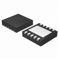
LTC3411EDD Linear Technology, LTC3411EDD Datasheet - Page 9

LTC3411EDD
Manufacturer Part Number
LTC3411EDD
Description
IC DC/DC CONV STEP-DOWN 10DFN
Manufacturer
Linear Technology
Type
Step-Down (Buck)r
Datasheet
1.LTC3411EDDPBF.pdf
(24 pages)
Specifications of LTC3411EDD
Internal Switch(s)
Yes
Synchronous Rectifier
Yes
Number Of Outputs
1
Voltage - Output
0.8 ~ 5 V
Current - Output
1.25A
Frequency - Switching
1MHz
Voltage - Input
2.63 ~ 5.5 V
Operating Temperature
-40°C ~ 85°C
Mounting Type
Surface Mount
Package / Case
10-DFN
Lead Free Status / RoHS Status
Contains lead / RoHS non-compliant
Power - Output
-
Available stocks
Company
Part Number
Manufacturer
Quantity
Price
Company:
Part Number:
LTC3411EDD
Manufacturer:
LT
Quantity:
10 000
Part Number:
LTC3411EDD
Manufacturer:
LT/凌特
Quantity:
20 000
Part Number:
LTC3411EDD#PBF
Manufacturer:
LINEAR/凌特
Quantity:
20 000
Company:
Part Number:
LTC3411EDD#TRPBF
Manufacturer:
PANASONIC
Quantity:
23 000
Part Number:
LTC3411EDD#TRPBF
Manufacturer:
LT
Quantity:
20 000
APPLICATIONS INFORMATION
A general LTC3411 application circuit is shown in Figure 5.
External component selection is driven by the load require-
ment, and begins with the selection of the inductor L1.
Once L1 is chosen, C
Operating Frequency
Selection of the operating frequency is a tradeoff between
effi ciency and component size. High frequency operation
allows the use of smaller inductor and capacitor values.
Operation at lower frequencies improves effi ciency by
reducing internal gate charge losses but requires larger
inductance values and/or capacitance to maintain low
output ripple voltage.
The operating frequency, f
by an external resistor that is connected between the R
pin and ground. The value of the resistor sets the ramp
current that is used to charge and discharge an internal
timing capacitor within the oscillator and can be calculated
by using the following equation:
or can be selected using Figure 2.
The maximum usable operating frequency is limited by
the minimum on-time and the duty cycle. This can be
calculated as:
f
R
O(MAX)
T
=
9 78 10
.
≈ 6.67 • (V
•
11
( )
f
O
IN
OUT
−
and C
1 08
/ V
O
.
, of the LTC3411 is determined
IN(MAX)
( )
OUT
Ω
can be selected.
) (MHz)
4.5
4.0
3.5
3.0
2.5
2.0
1.0
1.5
0.5
0
0
T
A
= 25°C
Figure 2. Frequency vs R
500
T
R
T
(kΩ)
The minimum frequency is limited by leakage and noise
coupling due to the large resistance of R
Inductor Selection
Although the inductor does not infl uence the operat-
ing frequency, the inductor value has a direct effect on
ripple current. The inductor ripple current ΔI
with higher inductance and increases with higher V
V
Accepting larger values of ΔI
tances, but results in higher output voltage ripple, greater
core losses, and lower output current capability.
A reasonable starting point for setting ripple current is 40%
of maximum output current, or ΔI
The largest ripple current ΔI
voltage. To guarantee that the ripple current stays below a
specifi ed maximum, the inductor value should be chosen
according to the following equation:
The inductor value will also have an effect on Burst Mode
operation. The transition from low current operation
begins when the peak inductor current falls below a level
set by the burst clamp. Lower inductor values result in
1000
OUT
L
Δ =
=
:
I
L
f
V
O
T
3411 F02
OUT
•
V
f
Δ
1500
OUT
O
I
•
L
L
•
• 1
⎛
⎜
⎝
⎛
⎜
⎝
1
−
−
V
V
V
IN MAX
V
OUT
OUT
IN
(
L
⎞
⎟
⎠
L
occurs at the maximum input
allows the use of low induc-
)
⎞
⎟
⎠
L
= 0.4 • 1.25A = 500mA.
LTC3411
T
.
L
decreases
IN
3411fb
9
or


