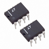
LT1302CN8-5 Linear Technology, LT1302CN8-5 Datasheet - Page 11

LT1302CN8-5
Manufacturer Part Number
LT1302CN8-5
Description
IC DC/DC CONV STEP-UP 5V 8-DIP
Manufacturer
Linear Technology
Type
Step-Up (Boost)r
Datasheet
1.LT1302CS8-5PBF.pdf
(16 pages)
Specifications of LT1302CN8-5
Internal Switch(s)
Yes
Synchronous Rectifier
No
Number Of Outputs
1
Voltage - Output
5V
Current - Output
600mA
Frequency - Switching
220kHz
Voltage - Input
2 ~ 8 V
Operating Temperature
0°C ~ 70°C
Mounting Type
Through Hole
Package / Case
8-DIP (0.300", 7.62mm)
Power - Output
700mW
Lead Free Status / RoHS Status
Contains lead / RoHS non-compliant
Available stocks
Company
Part Number
Manufacturer
Quantity
Price
Part Number:
LT1302CN8-5#PBF
Manufacturer:
LINEAR/凌特
Quantity:
20 000
APPLICATIONS
ally reaches audio frequencies, but at a much lighter load
than without the I
current combinations, some residual bursting may occur
at frequencies out of the audio band.
I
AC COUPLED
LOAD
100mV/DIV
INDUCTOR
Figure 8c. 3.3k Resistor for I
Efficiency at Moderate Load, Decreases at Light Load
CURRENT
Figure 8b. 3.3k Resistor from I
LT1302 into Current Mode Regardless of Load. Audio
Frequency Component Eliminated
1A/DIV
525mA
25mA
V
OUT
90
80
70
60
50
40
30
1
T
V
U
OUT
V
feature. At some input voltage/load
I
IN
T
FLOATING
INFORMATION
OUTPUT CURRENT (mA)
U
10
L1
3.3k I
1ms/DIV
D1
T
TO GND
T
C2
to Ground Increases
W
T
Figure 9. Suggested Component Placement for LT1302
Pin to Ground Forces
100
+
C1
2
R3
GND (BATTERY AND LOAD RETURN)
1302 F08c
1302 F08b
1000
U
C3
5
6
7
8
LT1302
The I
connected to the pin will cause erratic operation. If oper-
ating the device in Burst Mode, let the pin float. Keep high
dV/dt signals away from the pin.
Figure 8c details efficiency with and without the addition of
R1. Burst Mode operation keeps efficiency high at light
load with I
R1 added because the LT1302 cannot transition into Burst
Mode.
Layout
The high speed, high current switching associated with
the LT1302 mandates careful attention to layout. Follow
the suggested component placement in Figure 9 for proper
operation. High current functions are separated by the
package from sensitive control functions. Feedback resis-
tors R1 and R2 should be close to the feedback pin (pin4).
Noise can easily be coupled into this pin if care is not taken.
A small capacitor (100pF to 200pF) from FB to ground
provides a high frequency bypass. If the LT1302 is oper-
ated off a three-cell or higher input, R3 (2 to 10 ) in
series with V
from noise spikes on the input supply. Do not put in R3 if
the device must operate from a 2V input, as input current
will cause the voltage at the LT1302’s V
2V. The 0.1 F ceramic bypass capacitor C3 (use X7R, not
Z5U) should be mounted as close as possible to the
package. When R3 is used, C3 should be a 1 F tantalum
unit. Grounding should be segregated as illustrated. C3’s
ground trace should not carry switch current. Run a
T
pin cannot be used as a soft-start. Large capacitors
4
3
2
1
T
R1
floating. Efficiency falls off at light load with
IN
is recommended. This isolates the device
200pF
R
C
R2
SHUTDOWN
LT1302/LT1302-5
C
C
1302 F09
IN
pin to go below
11


