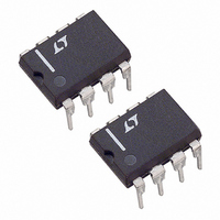
LT1302CN8-5 Linear Technology, LT1302CN8-5 Datasheet - Page 6

LT1302CN8-5
Manufacturer Part Number
LT1302CN8-5
Description
IC DC/DC CONV STEP-UP 5V 8-DIP
Manufacturer
Linear Technology
Type
Step-Up (Boost)r
Datasheet
1.LT1302CS8-5PBF.pdf
(16 pages)
Specifications of LT1302CN8-5
Internal Switch(s)
Yes
Synchronous Rectifier
No
Number Of Outputs
1
Voltage - Output
5V
Current - Output
600mA
Frequency - Switching
220kHz
Voltage - Input
2 ~ 8 V
Operating Temperature
0°C ~ 70°C
Mounting Type
Through Hole
Package / Case
8-DIP (0.300", 7.62mm)
Power - Output
700mW
Lead Free Status / RoHS Status
Contains lead / RoHS non-compliant
Available stocks
Company
Part Number
Manufacturer
Quantity
Price
Part Number:
LT1302CN8-5#PBF
Manufacturer:
LINEAR/凌特
Quantity:
20 000
OPERATIO
BLOCK DIAGRA
LT1302/LT1302-5
The LT1302’s operation can best be understood by
examining the block diagram in Figure 2. The LT1302
operates in one of two modes, depending on load. With
light loads, comparator CMP1 controls the output; with
heavy loads, control is passed to error amplifier A1.
Burst Mode operation consists of monitoring the FB pin
voltage with hysteretic comparator CMP1. When the FB
voltage, related to the output voltage by external attenu-
ator R1 and R2, falls below the 1.24V reference voltage,
the oscillator is enabled. Switch Q4 alternately turns on,
causing current buildup in inductor L1, then turns off,
allowing the built-up current to flow into output capaci-
tor C3 via D1. As the output voltage increases, so does
the FB voltage; when it exceeds the reference plus
6
SHDN
3
SENSE
GND
4
1
U
R1
315k
R2
105k
REFERENCE
1.24V
SHUTDOWN
W
SM
V
15mV
OS
+
–
–
+
A1
CMP1
HYSTERETIC
COMPARATOR
ERROR
AMPLIFIER
Figure 3. LT1302-5 Block Diagram
V
ENABLE
IN
Q5
V
V
IN
6
2
C
2
A
OSCILLATOR
220kHz
CMP1’s hysteresis (about 5mV) CMP1 turns the oscilla-
tor off. In this mode, peak switch current is limited to
approximately 1A by A2, Q2, and Q3. Q2’s current, set at
34 A, flows through R5, causing A2’s negative input to
be 25mV lower than V
36mV below V
The remaining 11mV is generated by Q3’s current flow-
ing through R4. Emitter-area scaling sets Q3’s collector
current to 0.625% of switch Q4’s current. When Q4’s
current is 1A, Q3’s current is 6.25mA, creating an 11mV
drop across R4 which, added to R5’s 25mV drop, is
enough to trip A2.
When the output load is increased to the point where the
1A peak current cannot support the output voltage,
OFF
A2
V
Q1
IN
+
–
IN
Q2
5
I
for A2 to trip and turn off the oscillator.
T
300
36mV
BIAS
IN
A3
730
. This node must fall more than
R5
DRIVER
3.6k
Q3
R4
1.75
PGND
SW
7
8
Q4
160X
1302 F03


