LTC3458EDE#PBF Linear Technology, LTC3458EDE#PBF Datasheet - Page 15
LTC3458EDE#PBF
Manufacturer Part Number
LTC3458EDE#PBF
Description
IC CONV DC/DC SYNC BOOST 12DFN
Manufacturer
Linear Technology
Type
Step-Up (Boost)r
Datasheet
1.LTC3458EDE.pdf
(16 pages)
Specifications of LTC3458EDE#PBF
Internal Switch(s)
Yes
Synchronous Rectifier
Yes
Number Of Outputs
1
Voltage - Output
2 ~ 7.5 V
Current - Output
1.4A
Frequency - Switching
1.5MHz
Voltage - Input
1.5 ~ 6 V
Operating Temperature
-40°C ~ 85°C
Mounting Type
Surface Mount
Package / Case
12-DFN
Dc To Dc Converter Type
Step Up
Pin Count
12
Input Voltage
6V
Output Voltage
2 to 7.5V
Switching Freq
1.15MHz
Output Current
1.6A
Efficiency
93%
Package Type
DFN EP
Output Type
Adjustable
Switching Regulator
Yes
Mounting
Surface Mount
Input Voltage (min)
1.5V
Operating Temp Range
-40C to 85C
Operating Temperature Classification
Industrial
Primary Input Voltage
6V
No. Of Outputs
1
No. Of Pins
12
Operating Temperature Range
-40°C To +85°C
Msl
MSL 1 - Unlimited
Rohs Compliant
Yes
Lead Free Status / RoHS Status
Lead free / RoHS Compliant
Power - Output
-
Lead Free Status / Rohs Status
Compliant
Available stocks
Company
Part Number
Manufacturer
Quantity
Price


PACKAGE DESCRIPTIO
3.60 ±0.05
TOP MARK
2.20 ±0.05
APPLY SOLDER MASK TO AREAS THAT ARE NOT SOLDERED
(NOTE 6)
RECOMMENDED SOLDER PAD PITCH AND DIMENSIONS
PIN 1
0.200 REF
NOTE:
1. DRAWING PROPOSED TO BE A VARIATION OF VERSION
2. DRAWING NOT TO SCALE
3. ALL DIMENSIONS ARE IN MILLIMETERS
4. DIMENSIONS OF EXPOSED PAD ON BOTTOM OF PACKAGE DO NOT INCLUDE
5. EXPOSED PAD SHALL BE SOLDER PLATED
6. SHADED AREA IS ONLY A REFERENCE FOR PIN 1 LOCATION
MOLD FLASH. MOLD FLASH, IF PRESENT, SHALL NOT EXCEED 0.15mm ON ANY SIDE
ON THE TOP AND BOTTOM OF PACKAGE
(WGED) IN JEDEC PACKAGE OUTLINE M0-229
1.70 ± 0.05
0.25 ± 0.05
Information furnished by Linear Technology Corporation is believed to be accurate and reliable.
However, no responsibility is assumed for its use. Linear Technology Corporation makes no represen-
tation that the interconnection of its circuits as described herein will not infringe on existing patent rights.
4.00 ±0.10
3.30 ±0.05
(2 SIDES)
2.50 REF
U
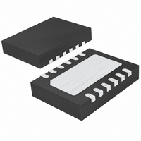
12-Lead Plastic DFN (4mm × 3mm)
0.50 BSC
(Reference LTC DWG # 05-08-1695)
0.70 ±0.05
0.75 ±0.05
3.00 ±0.10
(2 SIDES)
DE/UE Package
PACKAGE OUTLINE
0.00 – 0.05
R = 0.05
TYP
BOTTOM VIEW—EXPOSED PAD
1.70 ± 0.10
0.25 ± 0.05
6
7
R = 0.115
3.30 ±0.10
2.50 REF
TYP
0.50 BSC
12
1
0.40 ± 0.10
PIN 1 NOTCH
R = 0.20 OR
0.35 × 45°
CHAMFER
(UE12/DE12) DFN 0806 REV D
LTC3458
15
3458fa
Related parts for LTC3458EDE#PBF
Image
Part Number
Description
Manufacturer
Datasheet
Request
R

Part Number:
Description:
CD ROM LINEARVIEW DATASHEETS
Manufacturer:
Linear Technology

Part Number:
Description:
Standalone Linear Li-Ion Battery Charger with Thermal Regulation in ThinSOT
Manufacturer:
Linear Technology Corporation
Datasheet:
Part Number:
Description:
Low noise, high frequency, 8th order linear phase lowpass filter
Manufacturer:
Linear Technology Corporation
Datasheet:
Part Number:
Description:
Manufacturer:
Linear Technology Corporation
Datasheet:
Part Number:
Description:
Manufacturer:
Linear Technology Corporation
Datasheet:
Part Number:
Description:
Manufacturer:
Linear Technology Corporation
Datasheet:
Part Number:
Description:
Manufacturer:
Linear Technology Corporation
Datasheet:
Part Number:
Description:
Manufacturer:
Linear Technology Corporation
Datasheet:
Part Number:
Description:
Manufacturer:
Linear Technology Corporation
Datasheet:
Part Number:
Description:
Manufacturer:
Linear Technology Corporation
Datasheet:
Part Number:
Description:
Dual and Quad, JFET Input Precision High Speed Op Amps
Manufacturer:
Linear Technology Corporation
Datasheet:
Part Number:
Description:
Manufacturer:
Linear Technology Corporation
Datasheet:
Part Number:
Description:
1, 2, 6 and 8 Channel, 10-Bit Serial I/O Data Acquisition Systems
Manufacturer:
Linear Technology Corporation
Datasheet:
Part Number:
Description:
Manufacturer:
Linear Technology Corporation
Datasheet:
Part Number:
Description:
Universal dual filter building block
Manufacturer:
Linear Technology Corporation
Datasheet: