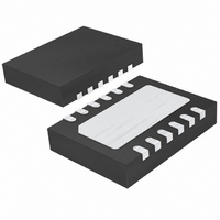
LTC3458EDE#PBF Linear Technology, LTC3458EDE#PBF Datasheet - Page 9

LTC3458EDE#PBF
Manufacturer Part Number
LTC3458EDE#PBF
Description
IC CONV DC/DC SYNC BOOST 12DFN
Manufacturer
Linear Technology
Type
Step-Up (Boost)r
Datasheet
1.LTC3458EDE.pdf
(16 pages)
Specifications of LTC3458EDE#PBF
Internal Switch(s)
Yes
Synchronous Rectifier
Yes
Number Of Outputs
1
Voltage - Output
2 ~ 7.5 V
Current - Output
1.4A
Frequency - Switching
1.5MHz
Voltage - Input
1.5 ~ 6 V
Operating Temperature
-40°C ~ 85°C
Mounting Type
Surface Mount
Package / Case
12-DFN
Dc To Dc Converter Type
Step Up
Pin Count
12
Input Voltage
6V
Output Voltage
2 to 7.5V
Switching Freq
1.15MHz
Output Current
1.6A
Efficiency
93%
Package Type
DFN EP
Output Type
Adjustable
Switching Regulator
Yes
Mounting
Surface Mount
Input Voltage (min)
1.5V
Operating Temp Range
-40C to 85C
Operating Temperature Classification
Industrial
Primary Input Voltage
6V
No. Of Outputs
1
No. Of Pins
12
Operating Temperature Range
-40°C To +85°C
Msl
MSL 1 - Unlimited
Rohs Compliant
Yes
Lead Free Status / RoHS Status
Lead free / RoHS Compliant
Power - Output
-
Lead Free Status / Rohs Status
Compliant
Available stocks
Company
Part Number
Manufacturer
Quantity
Price
APPLICATIO S I FOR ATIO
Error Amp. The error amplifier is a transconductance type,
with its positive input internally connected to the 1.23V
reference, and its negative input connected to FB. A simple
compensation network is placed from COMP to ground.
Internal clamps limit the minimum and maximum error
amp output voltage for improved large signal transient
response. During sleep (in Burst Mode), the compensa-
tion pin is high impedance, however clamps limit the
voltage on the external compensation network, preventing
the compensation capacitor from discharging to zero
during the sleep time.
Oscillator. The frequency of operation is set through a
resistor from R
capacitor resides inside the IC. The oscillator frequency is
calculated using the following formula:
where f
The oscillator can be synchronized with an external clock
applied to the SYNC pin. When synchronizing the oscilla-
tor, the free running frequency must be set to approxi-
mately 30% lower than the desired synchronized fre-
quency.
Soft-Start. The soft-start time is programmed with an
external capacitor to ground on SS. An internal current
source charges it with a nominal 5μA. The voltage on the
SS pin (in conjunction with the external resistor on I
used to control the peak current limit until the voltage on
the capacitor exceeds ~1V, at which point the external
resistor sets the peak current. In the event of a com-
manded shutdown, severe short-circuit, or a thermal
shutdown, the capacitor is discharged automatically.
Other LTC3458 Features and Functions
Antiringing Control. The antiringing control places a
resistor across the inductor to damp the ringing on SW pin
discontinuous conduction mode. The LC ringing
(L = inductor, C
but can cause EMI radiation.
t
f
(msec)
OSC
OSC
=
= C
0 2 0 004
is in MHz and R
.
SS
+
SW
T
(μF) • 200
to ground. An internally trimmed timing
.
= Capacitance on SW pin) is low energy,
1
U
•
R
T
U
T
is in kΩ
W
U
LIM
) is
Current Sensing. Lossless current sensing converts the
peak current signal to a voltage to sum in with the internal
slope compensation. This summed signal is compared to
the error amplifier output to provide a peak current control
command for the PWM. The slope compensation in the IC
is adaptive to the input and output voltage, therefore the
converter provides the proper amount of slope compensa-
tion to ensure stability, but not an excess to cause a loss
of phase margin in the converter.
Output Disconnect and Inrush Limiting. The LTC3458 is
designed to allow true output disconnect by eliminating
body diode conduction of the internal P-channel MOSFET
rectifier. This allows V
shutdown, drawing no current from the input source. It
also allows for inrush current limiting at turn-on, minimiz-
ing surge currents seen by the input supply. Note that to
obtain the advantages of output disconnect, there must be
no external Schottky diodes connected between SW and
V
Shutdown. The part is shut down by pulling SHDN below
0.3V, and made active by pulling the pin above 1.25V. Note
that SHDN can be driven above V
is limited to less than 8V.
Synchronous Rectifier. To prevent the inductor current
from running away, the P-channel MOSFET synchronous
rectifier is only enabled when V
Thermal Shutdown. If the die temperature reaches ap-
proximately 150°C, the part will go into thermal shutdown
and all switches will be turned off and the soft-start
capacitor will be reset. The part will be enabled again when
the die temperature has dropped by 10°C (nominal).
Zero Current Amplifier. The zero current amplifier moni-
tors the inductor current to the output and shuts off the
synchronous rectifier once the current is below 50mA
typical, preventing negative inductor current.
Burst Mode Operation
Burst Mode operation can be automatic or user controlled.
In automatic operation, the IC will automatically enter
Burst Mode operation at light load and return to fixed
frequency PWM mode for heavier loads. The user can
program the average load current at which the mode
OUT
.
0UT
to go to zero volts during
OUT
IN
or V
> (V
LTC3458
OUT
IN
+ 0.25V).
, as long as it
3458fa
9


