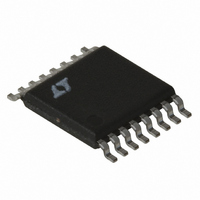
LT3825EFE#TRPBF Linear Technology, LT3825EFE#TRPBF Datasheet - Page 7

LT3825EFE#TRPBF
Manufacturer Part Number
LT3825EFE#TRPBF
Description
IC CNTRLR SYNC 16-TSSOP
Manufacturer
Linear Technology
Type
Flybackr
Datasheet
1.LT3825EFEPBF.pdf
(32 pages)
Specifications of LT3825EFE#TRPBF
Internal Switch(s)
No
Synchronous Rectifier
Yes
Number Of Outputs
1
Frequency - Switching
50kHz ~ 250kHz
Voltage - Input
12 ~ 18 V
Operating Temperature
-40°C ~ 125°C
Mounting Type
Surface Mount
Package / Case
16-TSSOP Exposed Pad, 16-eTSSOP, 16-HTSSOP
Power - Output
60W
Lead Free Status / RoHS Status
Lead free / RoHS Compliant
Current - Output
-
Voltage - Output
-
Available stocks
Company
Part Number
Manufacturer
Quantity
Price
V
switcher control loop. It is the output of the feedback
amplifier and the input to the current comparator. Switcher
frequency compensation components are normally placed
on this pin to ground. The voltage on this pin is propor-
tional to the peak primary switch current. The feedback
amplifier output is enabled during the synchronous
switch-on time.
UVLO (Pin 10): A resistive divider from V
an undervoltage lockout based upon V
When the UVLO pin is below its threshold, the gate drives
are disabled, but the part draws its normal quiescent current
from V
function so V
The bias current on this pin has hysteresis such that the
bias current is sourced when the UVLO threshold is ex-
ceeded. This introduces a hysteresis at the pin equivalent
to the bias current change times the impedance of the
upper divider resistor. The user can control the amount of
hysteresis by adjusting the impedance of the divider. See
the Applications Information for details. Tie the UVLO pin
to V
SENSE
to measure primary-side switch current through an ex-
ternal sense resistor. Peak primary-side current is used
in the converter control loop. Make Kelvin connections
to the sense resistor to reduce noise problems. SENSE
PIN FUNCTIONS
C
(Pin 9): Pin used for frequency compensation for the
CC
CC
if you are not using this function.
–
(Pin 11), SENSE
. The V
CC
CC
must be great enough to start the part.
undervoltage lockout supersedes this
+
(Pin 12): These pins are used
IN
IN
level (not V
to this pin sets
CC
).
–
connects to the ground side. At maximum current (V
its maximum voltage) it has a 98mV threshold. The signal
is blanked (ignored) during the minimum turn-on time.
C
optional load compensation function. Load compensation
reduces the effects of parasitic resistances in the feedback
sensing path. A 0.1μF ceramic capacitor suffices for most
applications. Short this pin to GND in less demanding ap-
plications that don’t require load compensation.
R
resistor. Use of this pin allows for nominal compensation
of parasitic resistances in the feedback sensing path. In
less demanding applications, this resistor is not needed
and this pin can be left open. See Applications Informa-
tion for details.
PGDLY (Pin 15): Pin for external programming resistor to
set delay from synchronous gate turn-off to primary gate
turn-on. See Applications Information for details.
PG (Pin 16): Gate Drive Pin for the Primary-Side MOSFET
Switch. Large dynamic currents flow during voltage transi-
tions. See the Applications Information for details.
GND (Exposed Pad Pin 17): This is the ground connection
for both signal ground and gate driver grounds. This GND
should be connected to the PCB ground plane. Careful at-
tention must be paid to ground layout. See Applications
Information for details.
CMP
CMP
(Pin 14): Pin for optional external load compensation
(Pin 13): Pin for external filter capacitor for the
LT3825
3825fc
7
C
at


