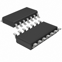
LTC1148LCS Linear Technology, LTC1148LCS Datasheet - Page 10

LTC1148LCS
Manufacturer Part Number
LTC1148LCS
Description
IC SW REG STEP-DWN HI-EFF 14SOIC
Manufacturer
Linear Technology
Type
Step-Down (Buck)r
Datasheet
1.LTC1148CSPBF.pdf
(20 pages)
Specifications of LTC1148LCS
Internal Switch(s)
No
Synchronous Rectifier
Yes
Number Of Outputs
1
Voltage - Output
Adjustable
Current - Output
50mA
Frequency - Switching
250kHz
Voltage - Input
3.5 ~ 20 V
Operating Temperature
0°C ~ 70°C
Mounting Type
Surface Mount
Package / Case
14-SOIC (3.9mm Width), 14-SOL
Lead Free Status / RoHS Status
Contains lead / RoHS non-compliant
Power - Output
-
Available stocks
Company
Part Number
Manufacturer
Quantity
Price
Part Number:
LTC1148LCS
Manufacturer:
LT/凌特
Quantity:
20 000
Company:
Part Number:
LTC1148LCS-3.3
Manufacturer:
Linear Technology
Quantity:
135
Part Number:
LTC1148LCS-3.3
Manufacturer:
LINEAR/凌特
Quantity:
20 000
Part Number:
LTC1148LCS-3.3#PBF
Manufacturer:
LINEAR/凌特
Quantity:
20 000
APPLICATIO S I FOR ATIO
LTC1148
LTC1148-3.3/LTC1148-5
level threshold MOSFETs (V
recommended. The LTC1148/LTC1148HV series supply
voltage must always be less than the absolute maximum
V
The maximum output current I
requirement for the two MOSFETs. When the LTC1148
series is operating in continuous mode, the simplifying
assumption can be made that one of the two MOSFETs is
always conducting the average load current. The duty
cycles for the two MOSFETs are given by:
From the duty cycles the required R
FET can be derived:
where P
d
P
requirements (see Efficiency Considerations). (1 + d) is
generally given for a MOSFET in the form of a normalized
R
used as an approximation for low voltage MOSFETs.
The Schottky diode D1 shown in Figure 1 only conducts
during the dead-time between the conduction of the two
power MOSFETs. D1’s sole purpose in life is to prevent the
body diode of the N-channel MOSFET from turning on and
storing charge during the dead time, which could cost as
much as 1% in efficiency (although there are no other
harmful effects if D1 is omitted). Therefore, D1 should be
selected for a forward voltage of less than 0.7V when
conducting I
10
P
GS
P
DS(ON)
P-Ch R
N-Ch R
P-Ch Duty Cycle =
N-Ch Duty Cycle =
and d
and P
ratings for the MOSFETs.
P
N
vs temperature curve, but d = 0.007/°C can be
N
and P
DS(ON)
DS(ON)
will be determined by efficiency and/or thermal
are the temperature dependencies of R
MAX
N
.
are the allowable power dissipations and
=
=
U U
V
(V
OUT
IN
V
(V
V
OUT
IN
IN
(I
– V
V
MAX
V
– V
IN
GS(TH)
OUT
IN
MAX
(P
V
OUT
2
)(1 + δ
IN
P
)(I
determines the R
)
(P
)
DS(ON)
MAX
< 2.5V) are strongly
W
N
)
P
2
)(1 + δ
)
for each MOS-
N
U
)
DS(ON)
DS(ON)
.
C
In continuous mode, the source of the P-channel MOSFET
is a square wave of duty cycle V
voltage transients, a low ESR input capacitor sized for the
maximum RMS current must be used. The maximum
RMS capacitor current is given by:
This formula has a maximum at V
I
monly used for design because even significant devia-
tions do not offer much relief. Note that capacitor
manufacturer’s ripple current ratings are often based on
only 2000 hours of life. This makes it advisable to further
derate the capacitor, or to choose a capacitor rated at a
higher temperature than required. Always consult the
manufacturer if there is any question. An additional 0.1µF
to 1µF ceramic capacitor is also required on V
high frequency decoupling.
The selection of C
series resistance (ESR). The ESR of C
than twice the value of R
LTC1148 series:
Optimum efficiency is obtained by making the ESR equal
to R
efficiency degrades by less than 1%. If the ESR is greater
than 2R
will prematurely trigger Burst Mode operation, resulting in
disruption of continuous mode and an efficiency hit which
can be several percent.
Manufacturers such as Nichicon and United Chemicon
should be considered for high performance capacitors.
The OS-CON semiconductor dielectric capacitor available
from Sanyo has the lowest ESR/size ratio of any aluminum
electrolytic at a somewhat higher price. Once the ESR
requirement for C
rating generally far exceeds the I
RMS
IN
C
C
and C
SENSE
IN
OUT
= I
Required I
OUT
SENSE
Required ESR < 2R
OUT
. As the ESR is increased up to 2R
/2. This simple worst-case condition is com-
, the voltage ripple on the output capacitor
Selection
RMS
OUT
OUT
is driven by the required effective
has been met, the RMS current
≈ I
SENSE
MAX
SENSE
for proper operation of the
[V
OUT
RIPPLE(P-P)
OUT
/V
IN
IN
(V
OUT
. To prevent large
IN
= 2V
V
– V
IN
must be less
requirement.
OUT
IN
OUT
SENSE
Pin 3 for
, where
)]
114835fd
1/2
, the


