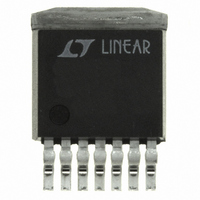
LT1506CR-SYNC Linear Technology, LT1506CR-SYNC Datasheet - Page 19

LT1506CR-SYNC
Manufacturer Part Number
LT1506CR-SYNC
Description
IC SW REG STEP-DOWN 500KHZ 7-DD
Manufacturer
Linear Technology
Type
Step-Down (Buck)r
Datasheet
1.LT1506CS8-3.3PBF.pdf
(24 pages)
Specifications of LT1506CR-SYNC
Internal Switch(s)
Yes
Synchronous Rectifier
No
Number Of Outputs
1
Voltage - Output
Adjustable
Current - Output
4.5A
Frequency - Switching
500kHz
Voltage - Input
4 ~ 15 V
Operating Temperature
0°C ~ 125°C
Mounting Type
Surface Mount
Package / Case
D²Pak, TO-263 (7 leads + tab)
Lead Free Status / RoHS Status
Contains lead / RoHS non-compliant
Power - Output
-
Available stocks
Company
Part Number
Manufacturer
Quantity
Price
Part Number:
LT1506CR-SYNC
Manufacturer:
LINEAR/凌特
Quantity:
20 000
Part Number:
LT1506CR-SYNC#TRPBF
Manufacturer:
LINEAR/凌特
Quantity:
20 000
APPLICATIONS
Error amplifier transconductance phase and gain are shown
in Figure 11. The error amplifier can be modeled as a
transconductance of 2000 Mho, with an output imped-
ance of 200k
applications, the compensation network from V
ground has a much lower impedance than the output
impedance of the amplifier at frequencies above 500Hz.
This means that the error amplifier characteristics them-
selves do not contribute excess phase shift to the loop, and
the phase/gain characteristics of the error amplifier sec-
tion are completely controlled by the external compensa-
tion network.
In Figure 12, full loop phase/gain characteristics are
shown with a compensation capacitor of 1.5nF, giving the
error amplifier a pole at 530Hz, with phase rolling off to 90
and staying there. The overall loop has a gain of 74dB at
low frequency, rolling off to unity-gain at 100kHz. Phase
shows a two-pole characteristic until the ESR of the output
capacitor brings it back above 10kHz. Phase margin is
about 60 at unity-gain.
Analog experts will note that around 4.4kHz, phase dips
very close to the zero phase margin line. This is typical of
switching regulators, especially those that operate over a
wide range of loads. This region of low phase is not a
problem as long as it does not occur near unity-gain. In
practice, the variability of output capacitor ESR tends to
dominate all other effects with respect to loop response.
Variations in ESR will cause unity-gain to move around,
but at the same time phase moves with it so that adequate
phase margin is maintained over a very wide range of ESR
(
3:1).
Figure 10. Response from V
–20
–40
40
20
0
10
in parallel with 12pF. In all practical
100
U
PHASE
GAIN
FREQUENCY (Hz)
1k
INFORMATION
U
10k
C
V
V
I
100k
W
OUT
IN
OUT
Pin to Output
= 10V
= 2A
= 5V
1505 F10
1M
40
0
–40
–80
–120
U
C
pin to
What About a Resistor in the Compensation Network?
It is common practice in switching regulator design to add
a “zero” to the error amplifier compensation to increase
loop phase margin. This zero is created in the external
network in the form of a resistor (R
compensation capacitor. Increasing the size of this resis-
tor generally creates better and better loop stability, but
there are two limitations on its value. First, the combina-
tion of output capacitor ESR and a large value for R
cause loop gain to stop rolling off altogether, creating a
gain margin problem. An approximate formula for R
where gain margin falls to zero is:
R Loop
C
Figure 11. Error Amplifier Gain and Phase
3000
2500
2000
1500
1000
500
Figure 12. Overall Loop Characteristics
–20
80
60
40
20
Gain = 1
100
0
10
V
R
ERROR AMPLIFIER EQUIVALENT CIRCUIT
V
V
C
C
FB 2 10
LOAD
IN
OUT
OUT
C
= 1.5nF, R
= 10V
= 5V, I
= 100 F, 10V, AVX TPS
1k
100
= 50
–3
OUT
FREQUENCY (Hz)
C
PHASE
FREQUENCY (Hz)
GAIN
= 0, L = 10 H
10k
= 2A
G
1k
MP
GAIN
R
200k
OUT
100k
10k
G
MA
V
OUT
1M
100k
C
12pF
PHASE
C
OUT
ESR
) in series with the
V
C
1506 F11
1505 F12
10M
1M
200
150
100
50
0
–50
2 42
200
150
100
50
0
–50
LT1506
19
C
may
C


